Substrate for liquid crystal display and liquid crystal display utilizing the same

a technology of liquid crystal display and substrate, which is applied in the direction of instruments, mechanical devices, operating means/releasing devices of valves, etc., can solve the problems of color filter coming off, low color purity, lack of contact between the pixel electrode and the tft, etc., to suppress the generation of flakes or residues, improve the display characteristics and reliability of the lcd manufactured utilizing the same, and prevent the occurrence of conduction failures

Active Publication Date: 2006-03-14
UNIFIED INNOVATIVE TECH
View PDF7 Cites 47 Cited by
  • Summary
  • Abstract
  • Description
  • Claims
  • Application Information

AI Technical Summary

Benefits of technology

[0019]In the case of such an LCD, since residues or flakes of color filters are unlikely to be generated on an LCD substrate, the occurrence of conduction failures is suppressed, and display characteristics and reliability of an LCD manufactured utilizing the same can be improved.
[0020]According to the invention, a passivation film formed between pixel electrodes and switching elements on an LCD substrate has a multi-layer structure constituted by a SiN layer and a SiO layer or a SiON layer, and a CF layer is in contact with the SiO layer or SiON layer. This makes it possible to suppress the generation of flakes or residues of the color filter and to thereby suppress the occurrence of conduction failures, and an LCD substrate and an LCD having high display characteristics and high reliability can therefore be provided.
[0021]Further, by adjusting the film thickness of the SiO layer or the SiON layer and the inner structure of the SiN layer, a contact hole formed in the passivation film can be provided with a forwardly tapered sectional configuration to provide an LCD substrate and an LCD having high performance without conduction failures.

Problems solved by technology

This has resulted in problems in that the color filters can come off the SiN surface when the resin CF layers are formed and in that residues of the resin CF layers after etching can remain in contact holes that extend up to the TFTs when the contact holes are formed.
Such residues or flakes of color filters can cause problems such as low color purity, and a resultant defect in the patterning of an electrode material formed in a contact hole can result in problems such as lack of contact between the pixel electrode and the TFT.

Method used


Image

  • Substrate for liquid crystal display and liquid crystal display utilizing the same
  • Substrate for liquid crystal display and liquid crystal display utilizing the same
  • Substrate for liquid crystal display and liquid crystal display utilizing the same

Examples


embodiment 1 — 1

Embodiment 1—1

[0052]First, Embodiment 1—1 will be described.

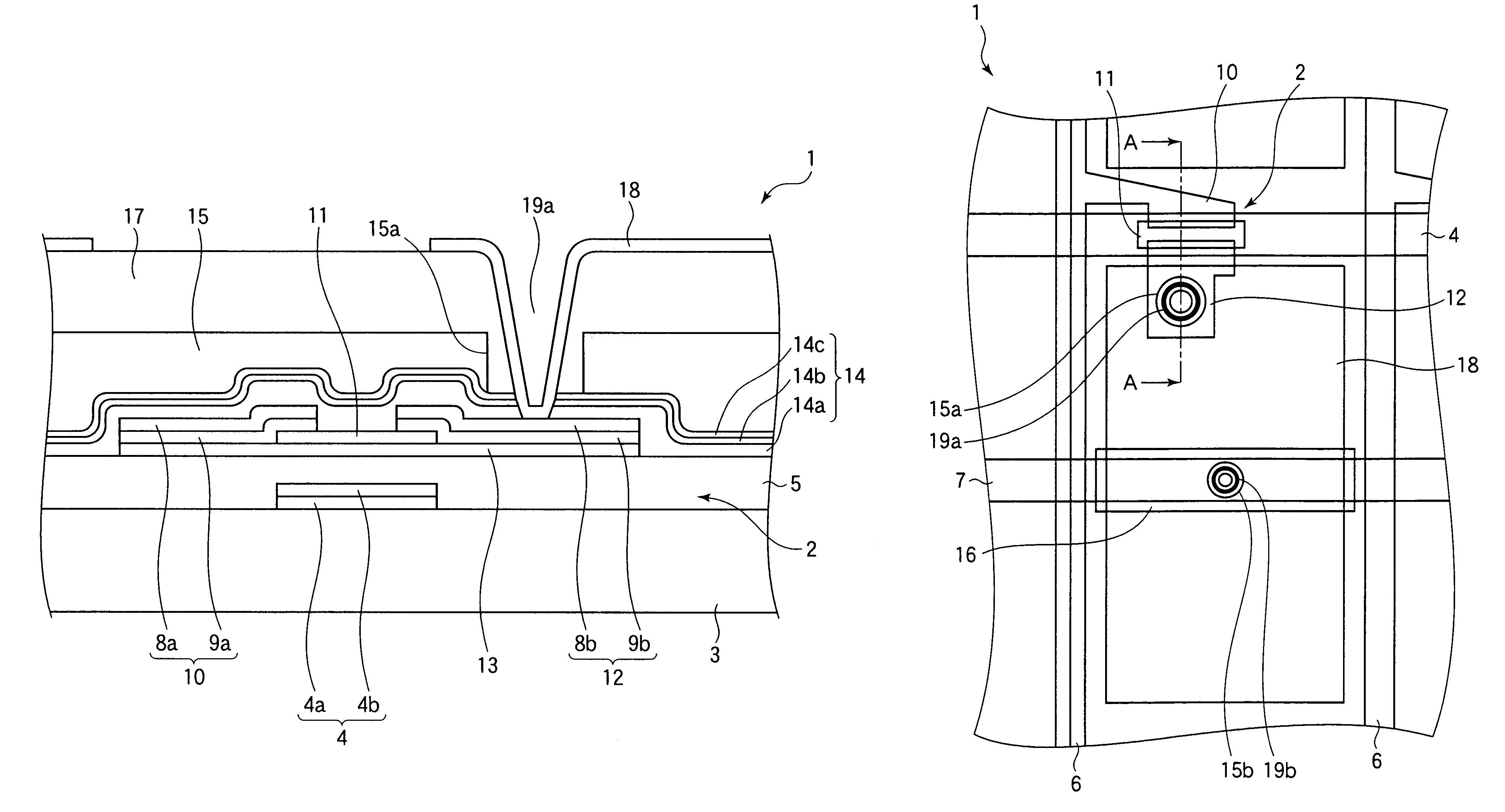
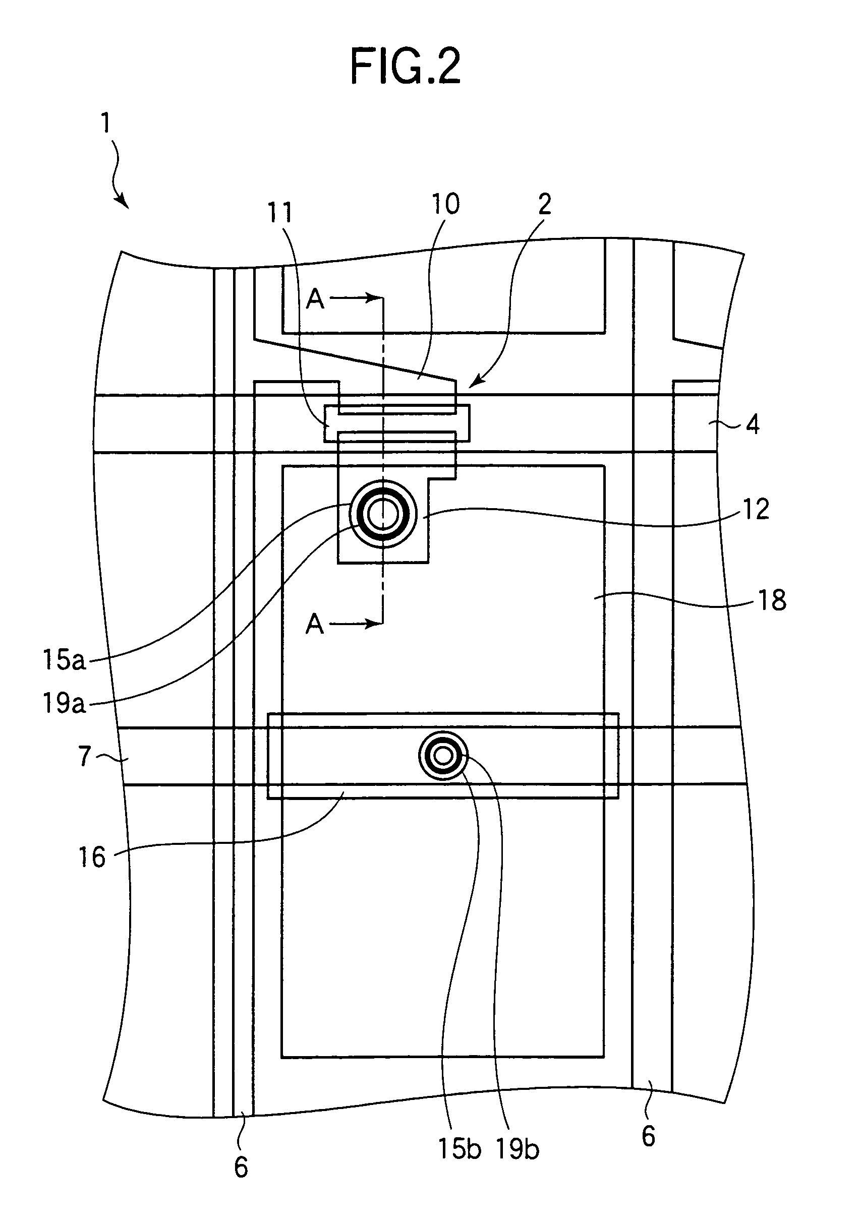
[0053]FIG. 1 is a sectional view of a major part of the region of a TFT on a TFT substrate according to Embodiment 1—1, and FIG. 2 is a plan view of one pixel region of the TFT substrate of Embodiment 1—1. FIG. 1 shows a section taken along the line A—A in FIG. 2. An LCD according to Embodiment 1—1 has a structure in which a TFT substrate 1 having TFTs 2 as shown in FIGS. 1 and 2 formed thereon as switching elements and an opposite substrate having a common electrode formed thereon are combined and in which a liquid crystal is enclosed between the substrates.

[0054]In the TFT substrate 1 used in such an LCD, layers 4b of a metal having a high melting point such as titanium (Ti), chromium (Cr) or molybdenum (Mo) are formed on a glass substrate 3 as a transparent insulated substrate with aluminum (Al) type metal layers 4a interposed therebetween to form a plurality of gate bus lines 4 (only one of which is shown in FIG. 2). An...

embodiment 1-2

[0078]Now, Embodiment 1-2 will be described below. While the passivation film 14 has the multi-layer structure constituted by the SiN layers 14a and 14b and the SiO layer 14c in the above-described Embodiment 1—1, the passivation film 14 formed on the TFT substrate 1 may have a multi-layer structure constituted by SiN layers 14a and 14b and a SiON layer. The SiON layer is preferably formed with a thickness in the range from 3 nm to 20 nm similarly to the above-described SiO layer 14c. The same effect as that of the SiO layer 14c can be provided by using a SiON layer instead of the SiO layer 14c in the passivation film 14. Similarly to the SiO layer 14c, the SiON layer can be formed using a plasma CVD process after the SiN layers 14a and 14b are formed. The SiON layer may be formed by forming an a-Si layer and thereafter performing at least one of an ashing process, high-pressure oxidation, thermal oxidation, a N2O plasma process and a N2+O2 plasma process on the same. Alternatively,...

embodiment 2-1

[0090]A description will now be made with reference to FIGS. 16 to 21B on a substrate for a liquid crystal display and a liquid crystal display having the same according to Embodiment 2-1. FIG. 16 shows a configuration of three pixels on a TFT substrate (base substrate) 1 of the present embodiment taken from above. FIGS. 17A and 17B show a section of a part of a red pixel of the TFT substrate 1. FIG. 17A shows a section of the TFT substrate 1 taken along the line A—A in FIG. 16, and FIG. 17B shows a section of the TFT substrate 1 taken along the line B—B in FIG. 16. As shown in FIG. 16, the TFT substrate 1 has a plurality of gate bus lines 4 (only one of which is shown in FIG. 16) extending on a glass substrate 3 in the horizontal direction in the figure and a plurality of drain bus lines 6 extending in the vertical direction in the figure such that they intersect with the gate bus lines 4 with an insulation film 5 interposed between them. Pixel regions are defined by the gate bus l...


PUM

PropertyMeasurementUnit
areaaaaaaaaaaa
thicknessaaaaaaaaaa
thicknessaaaaaaaaaa

Abstract

The generation of residues or flakes of a color filter is suppressed to eliminate conduction failures on an LCD substrate having a color filter on an array substrate. A passivation film formed between a pixel electrode formed in each of a plurality of pixel regions and a TFT for driving the pixel electrode has a multi-layer structure constituted by SiN layers and a SiO layers, and the SiO layer is located at the top of the film. A resin CF layer is formed on the passivation film having such a multi-layer structure. Since the resin CF layer is formed directly on the SiO layer, reduction of the adhesion of the same is suppressed. As a result, the color filter is unlikely to come off when the resin CF layer is formed, and residues of the color filter is unlikely to be generated when a contact hole is formed in the resin CF layer. This suppresses conduction failures and makes it possible to provide a reliable TFT substrate and LCD having high display characteristics.

Description

BACKGROUND OF THE INVENTION[0001]1. Field of the Invention[0002]The present invention relates to a substrate for a liquid crystal display and a liquid crystal display utilizing the same and, more particularly, to a substrate for a liquid crystal display in which color filters are formed on an array substrate having switching elements such as thin film transistors formed thereon and a liquid crystal display utilizing such a substrate for a liquid crystal display.[0003]2. Description of the Related Art[0004]Active matrix liquid crystal displays (LCDs) utilizing thin film transistors (TFTS) as switching elements that have been proposed in the past include inverted staggered structure TFT-LCDs (for example, see Japanese Patent Laid-Open No. JP-A-6-202153). In order to achieve greater aperture ratios, proposals have recently been made on LCDs utilizing an LCD substrate having a CF-on-TFT structure in which color filters are formed on an array substrate having switching elements such as T...

Claims


Application Information

Patent Timeline
Patent Type & Authority Patents(United States)
IPC IPC(8): G02F1/136G02F1/1335G02F1/1362G02F1/1368H01L29/786
CPCG02F1/136227G02F2001/136222G02F1/136222F16K31/0668F16K25/02F16K47/023
Inventor SAWASAKI, MANABUTANOSE, TOMONORIMISAKI, KATSUNORI
Owner UNIFIED INNOVATIVE TECH
Why Eureka
Try Eureka