Multi-layered barrier metal thin films for Cu interconnect by ALCVD

Inactive Publication Date: 2006-03-21
SHARP KK
View PDF4 Cites 5 Cited by
  • Summary
  • Abstract
  • Description
  • Claims
  • Application Information

AI Technical Summary

Benefits of technology

[0006]A multi-layered barrier metal thin film is deposited on a substrate by atomic layer chemical vapor deposition (ALCVD). The multi-layer film may comprise several different layers of a single chemical species, or several layers each of distinct or alternating chemical species. In a preferred embodiment, the multi-layer barrier thin film comprises a Tantalum Nitride (TaN) layer on a substrate with a Titanium Nitride (TiN) layer deposited thereon. The thickness of the entire multi-layer film is typically as small as fifty Angstroms. The film has superior film characteristics, such as anti-diffusion capability, low resistivity, high density, and step coverage, when compared to films deposited by conventional chemical vapor deposition (CVD). The multi-layered barrier metal thin film of the present invention has improved adhesion characteristics and is particularly suited for metallization of a Copper film thereon.
[0008]Another object of the invention is to provide a multi-layer barrier metal film, and a method of producing the same, having improved film characteristics.
[0010]Still a further object of the invention is to provide a multi-layer barrier metal film having improved adhesion characteristics for the metallization of a Copper film thereon.

Problems solved by technology

Conventional metal organic chemical vapor deposition (MOCVD), however, does not allow for the manufacture of films having a smaller thickness while having the same, or improved, film properties as thicker films.
However, due to the anisotropic nature of the plasma treatment, the film properties of the barrier metal film deposited on a side wall of a trench or a via are different from the film properties of the film deposited on the horizontal surfaces of the deposition surface.
Accordingly, current technology is limited with regard to the thickness to which barrier metal films can be reduced and with regard to the properties of barrier metal films.

Method used


Image

  • Multi-layered barrier metal thin films for Cu interconnect by ALCVD
  • Multi-layered barrier metal thin films for Cu interconnect by ALCVD
  • Multi-layered barrier metal thin films for Cu interconnect by ALCVD

Examples


Embodiment Construction

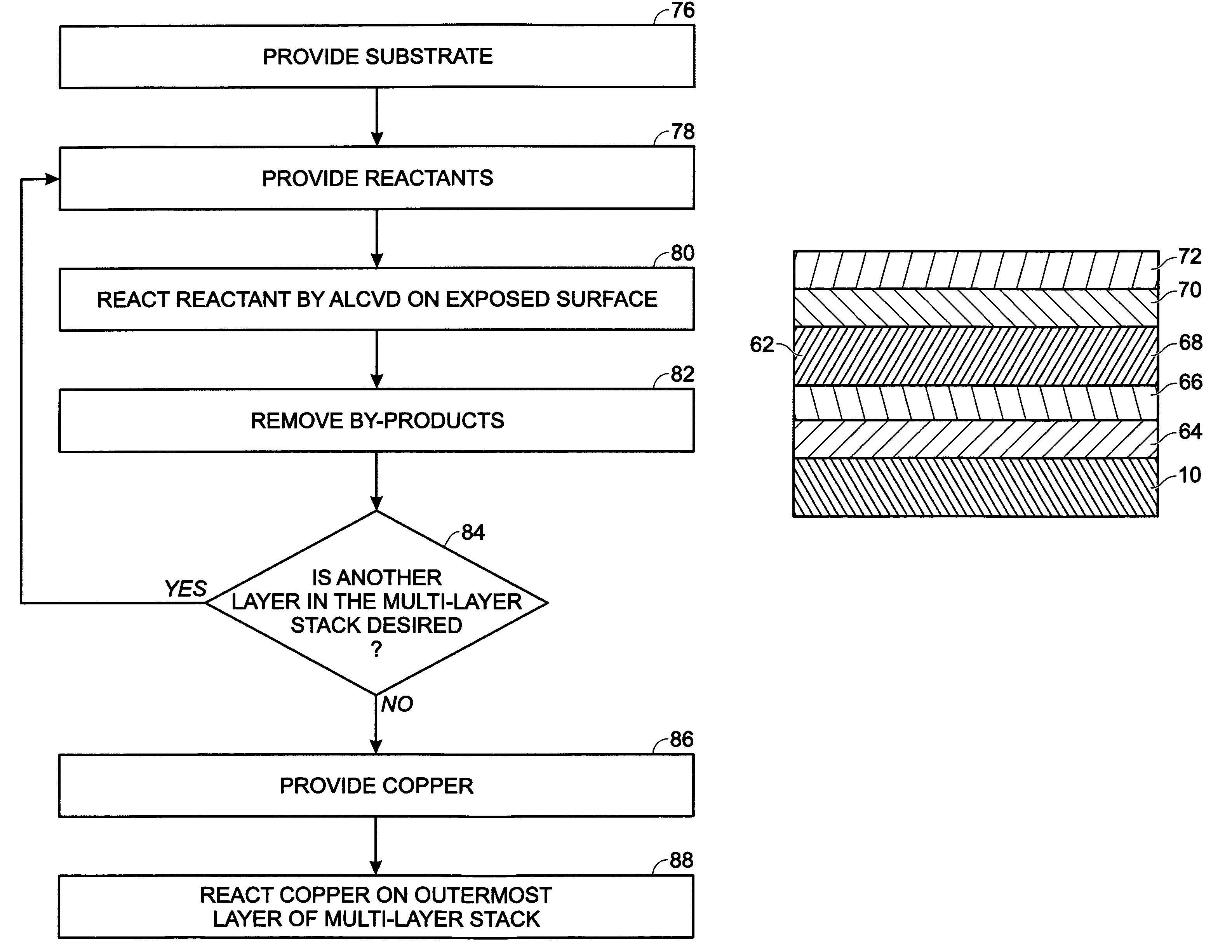
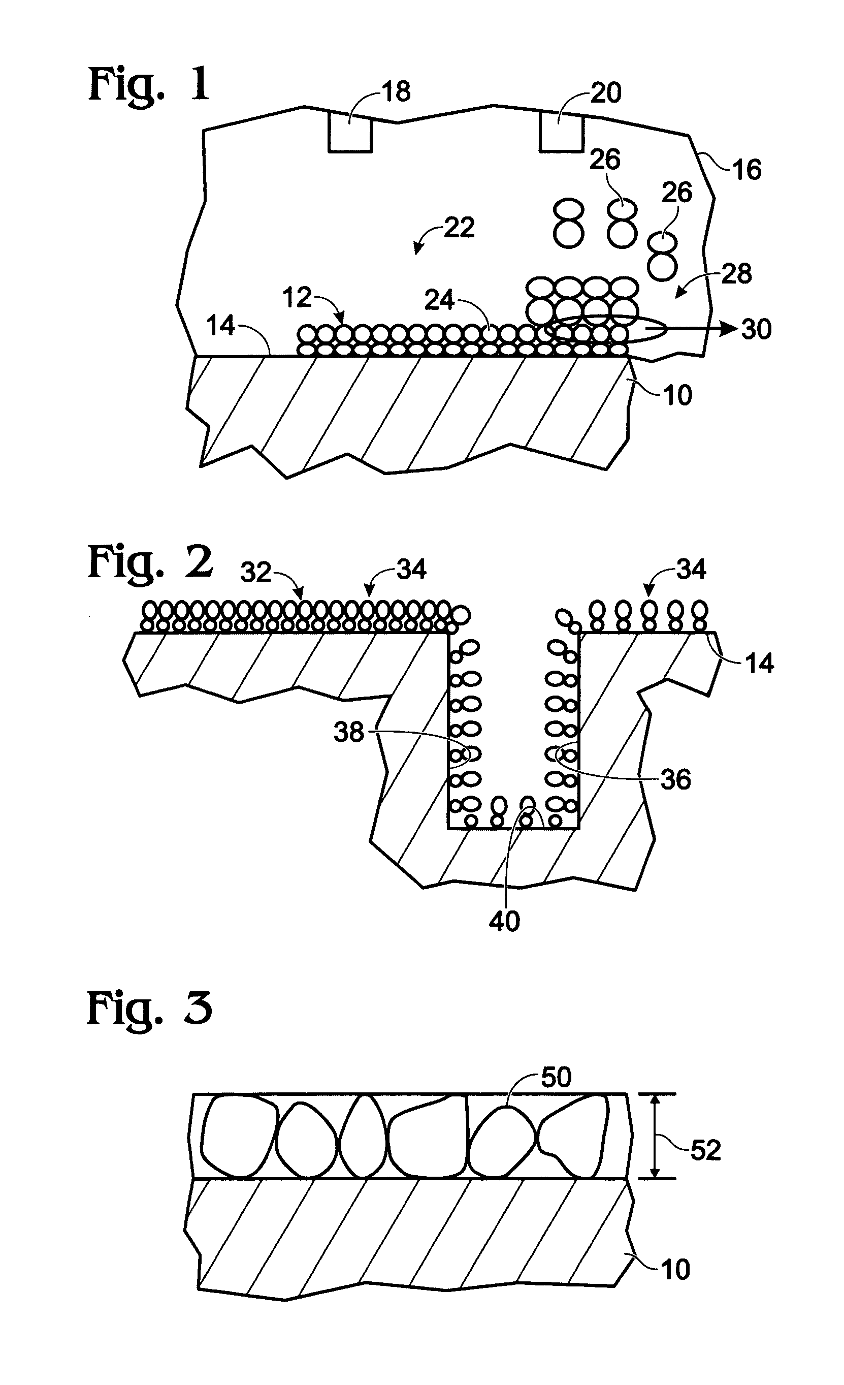
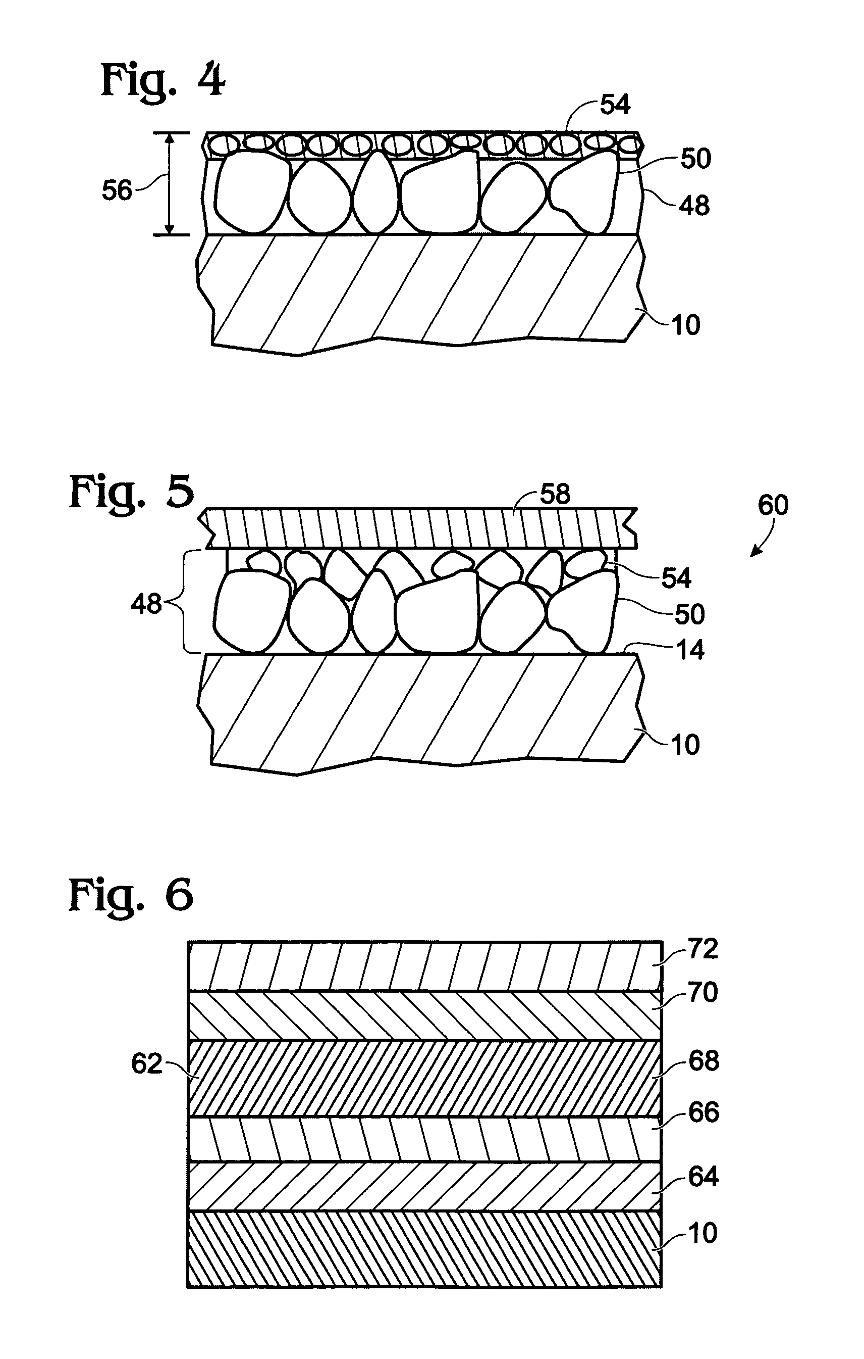
[0018]Atomic layer chemical vapor deposition (ALCVD) is an emerging technology that is being adopted in mainstream semiconductor research for eventual transfer to manufacturing. ALCVD uses fast operating valves to deliver individual reactants to a deposition chamber. Each reactant lays a mono-layer, i.e., an atomic layer, or several mono-layers, on the wafer structure through chemical adsorption and reacts with a previously deposited mono-layer species to form a desired compound. The as-formed compound will have a higher density than can be achieved by conventional CVD methods. The as-formed compound will also have excellent step coverage. By carefully selecting precursors, multi-layered or alternating layered barrier metal films are achievable. For example, alternating Tantalum Nitride / Silicon Nitride (TaN / SiN), Tantalum Nitride / Titanium Nitride (TaN / TiN) and Titanium Nitride / Silicon Nitride (TiN / SiN) thin films, or their combinations, are relatively easy to deposit using the ALCVD...


PUM

PropertyMeasurementUnit
Temperatureaaaaaaaaaa
Timeaaaaaaaaaa
Thicknessaaaaaaaaaa

Abstract

A multi-layered barrier metal thin film is deposited on a substrate by atomic layer chemical vapor deposition (ALCVD). The multi-layer film may comprise several different layers of a single chemical species, or several layers each of distinct or alternating chemical species. In a preferred embodiment, the multi-layer barrier thin film comprises a Tantalum Nitride layer on a substrate, with a Titanium Nitride layer deposited thereon. The thickness of the entire multi-layer film may be approximately fifty Angstroms. The film has superior film characteristics, such as anti-diffusion capability, low resistivity, high density, and step coverage, when compared to films deposited by conventional chemical vapor deposition (CVD). The multi-layered barrier metal thin film of the present invention has improved adhesion characteristics and is particularly suited for metallization of a Copper film thereon.

Description

FIELD OF THE INVENTION[0001]This invention relates to a multi-layered barrier metal thin film and a method of producing the same and, more particularly, to a multi-layered barrier metal thin film for copper interconnect wherein the multi-layered structure is manufactured by atomic layer chemical vapor deposition.BACKGROUND OF THE INVENTION[0002]In order to increase the speed of integrated circuit devices it is desired to manufacture the devices in as small a size as possible. By manufacturing the semiconductor devices with ever smaller sized features, the thickness of the barrier metal thin film for interconnect metallization within the device is also forced to be reduced.[0003]However, the properties of the barrier metal thin film, such as its anti-diffusion capability, low resistivity, high density, step coverage, and other such properties, are required to remain the same or even improve. Conventional metal organic chemical vapor deposition (MOCVD), however, does not allow for the...

Claims


Application Information

Patent Timeline
IPC IPC(8): H01L21/44C23C16/34H01L21/205H01L21/28H01L21/285H01L21/3205H01L21/768H01L23/52
CPCH01L21/28562H01L21/76841H01L2221/1078H01L21/76846H01L21/76877
Inventor PAN, WEIONO, YOSHIEVANS, DAVID R.HSU, SHENG TENG
Owner SHARP KK
Why Eureka
Try Eureka