Method of increasing CPP GMR in a spin valve structure

a technology of spin valve and gmr, which is applied in the field of giant magnetoresistive (gmr) magnetic field sensor fabrication, can solve the problems of loss of current (and sensitivity), adverse effects on the overall sensitivity of the sensor, and inability to meet the requirements of cpp configuration, etc., and achieves the retention of dr of such a stack, the effect of low resistance current and greatly reduced resultant resistan

Active Publication Date: 2006-03-21
HEADWAY TECH INC
View PDF14 Cites 20 Cited by
  • Summary
  • Abstract
  • Description
  • Claims
  • Application Information

AI Technical Summary

Benefits of technology

[0014]Accordingly, it is a first object of this invention is to provide a novel current-perpendicular-to-plane (CPP) giant magnetoresistive (GMR) read-sensor stack structure of a synthetic spin valve configuration, having decreased resistance and improved sensitivity.
[0015]It is a second object of this invention to provide a sensor stack structure wherein the current path through said sensor stack does not produce local hot spots due to increased Joule heating effects.
[0017]In contrast, there is shown in FIG. 2 the CPP structure to be formed in the present invention. That structure provides a low resistance current path by means of a novel design in which a ferromagnetic free layer (10) and Cu capping layer (12) of small dimension (<0.1 micron), is formed on a Cu spacer layer (20) of slightly larger dimension (approximately 0.3 microns) and that spacer layer is formed on a GMR stack (40) of synthetic spin valve configuration having equal, uniform layer dimensions that were larger that either of the above (>0.3 microns). The GMR stack includes a lead layer (42), a seed layer (44), an antiferromagnetic pinning layer (46), and a synthetic antiferromagnetic pinned layer (48), further comprising a second ferromagnetic layer (denoted AP2) (50), a coupling layer (52) and a first ferromagnetic layer (AP1) (54). The resultant resistance of such a stack is greatly reduced (as is also disclosed in related applications HT1 02-003, fully incorporated herein by reference) compared to the prior art stack of uniform dimension shown in FIG. 1. In addition, the DR of such a stack is retained, or even enhanced, with the use of the large Cu spacer layers (20), since the spin diffusion length of electrons in Cu (the distance an electron can travel with its spin direction unchanged) is approximately 1500 angstroms. Therefore, the DR of the sensor (resistance change between parallel and antiparallel orientations of free and pinned layer magnetizations) is not changed, but the total resistance, R, is significantly reduced, so the GMR sensitivity, DR / R is increased. It is also to be noted that the dimensional differentials between the free layer (10), the spacer layer (20) and the synthetic antiferromagnetic pinned layer (48) produces an angle to the current that effectively provides the electrons a greater path length within the coupled layers of the pinning layer and a corresponding improvement in DR. This is indicated in a graphical representation of the longitudinal current component in the ferromagnetic layers of the synthetic pinned layer. In addition, the current density in the pinned layer is reduced since the current is distributed over a greater cross-sectional area, thereby also reducing the current-induced magnetic field and relaxing the pinning strength requirement on the antiferromagnetic pinning layer. Finally, the reduced resistance and elimination of hot spots in the high resistance seed layer and pinning layer allows a greater sensor current to be applied, increasing signal strength and further improving the sensitivity of the sensor.

Problems solved by technology

Unfortunately, CIP GMR sensor configurations typically involve layer stacks comprising layers that are electrically conductive but not magnetically active and that play no role in providing resistance variations.
As a result, portions of the current are shunted through regions that produce no detectable responses and, thereby, the overall sensitivity of the sensor is adversely affected.
The CPP configuration is not without its problems, however.
The inherent problem in the CIP configuration is the loss of current (and sensitivity) through conductive, but non-magnetic layers; the analogous problem in the CPP configuration is the large voltage drop across magnetically inactive high resistance layers, which tends to mask the voltage variations produced by the active layers.
It is worth noting that the high value of R also increases Joule heating in the sensor, causes local hot-spots and, therefore, limits the allowable magnitude of the sensing current.
This would necessitate a difficult materials search.
The pertinent prior art cited below has offered no similar method for improving the sensitivity of the CPP design having a synthetic spin valve stack configuration.
Although the prior art described above provide methods for improving the performance attributes of GMR spin valves in a CPP configuration, they do not address the problem of the high resistance of an AFM pinning layer and seed layer and its adverse affect on sensor sensitivity.
In particular, the prior art does not discuss or disclose a method of forming such a CPP GMR sensor in which the geometry of the various layers permits a re-distribution of current within the sensor stack that effectively reduces its resistance and thereby increases it sensitivity.

Method used


Image

  • Method of increasing CPP GMR in a spin valve structure
  • Method of increasing CPP GMR in a spin valve structure
  • Method of increasing CPP GMR in a spin valve structure

Examples


Embodiment Construction

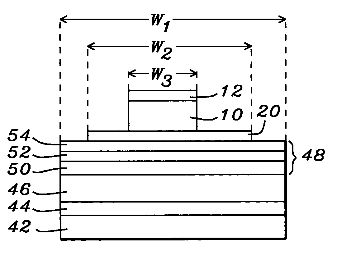
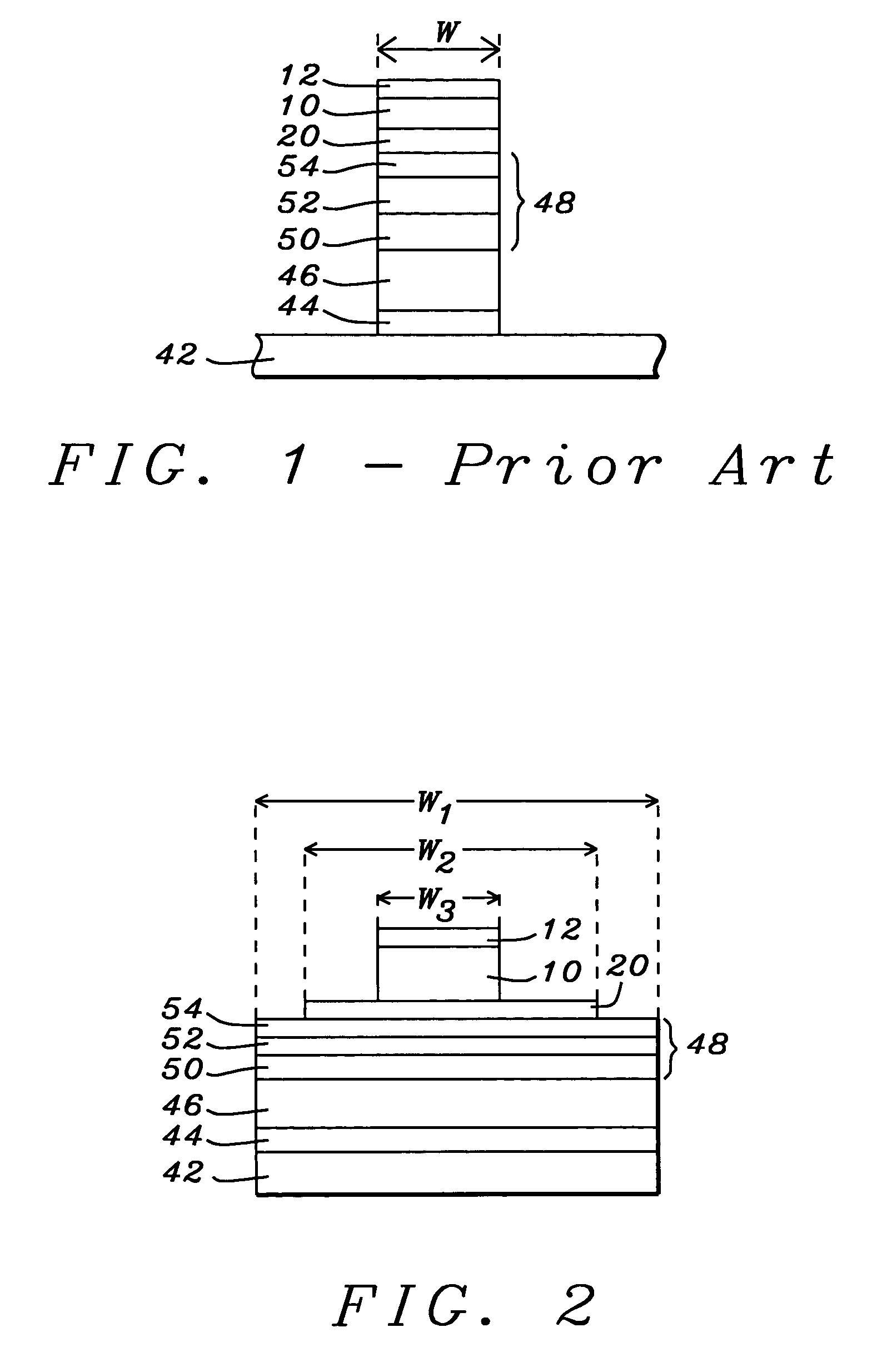
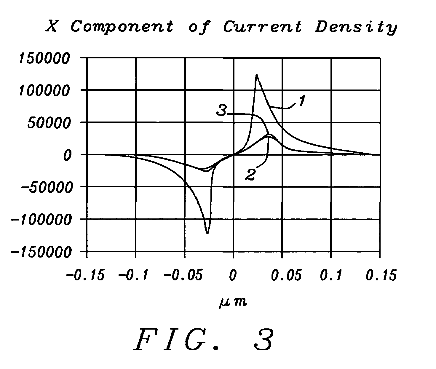
[0022]The present invention is a GMR spin valve sensor in a CPP (current-perpendicular-to-plane) synthetic pinned layer spin-valve configuration having a novel geometry that improves sensor sensitivity, DR / R, by maintaining (or improving) DR, while significantly reducing R. The novel design includes a ferromagnetic free layer of very small cross-sectional area, centered on a conducting, non-magnetic spacer layer of larger cross-sectional area, with the spacer layer then being centered on the remaining GMR sensor stack which is of still larger cross-sectional area. The step-wise reduction in cross-sectional areas of the layers leads to reduced current density in the pinned layer as well as a more longitudinal current path, both enhancing the performance of the sensor.

[0023]Referring again to FIG. 2, there is shown a schematic view of the CPP GMR spin valve sensor provided by the present invention. What will be referred to herein as the GMR stack comprises the following: a lead layer ...


PUM

PropertyMeasurementUnit
thicknessaaaaaaaaaa
thicknessaaaaaaaaaa
thicknessaaaaaaaaaa

Abstract

A current-perpendicular-to-plane (CPP) giant magnetoresistive (GMR) sensor of the synthetic spin valve type is provided, the sensor comprising a GMR stack having a substantially square lateral cross-section, a Cu spacer layer of smaller square cross-section formed centrally on the GMR stack and a capped ferromagnetic free layer of substantially square, but even smaller cross-sectional area, formed centrally on the spacer layer. The stepped, reduced area geometry of the sensor provides a significant improvement in its GMR ratio (DR / R), a reduced resistance, R, and elimination of Joule heating hot-spots in regions of high resistance such as the antiferromagnetic pinning layer and its seed layer.

Description

RELATED PATENT APPLICATION[0001]This application is related to Ser. No. 10 / 392,118, filing date Mar. 19, 2003 and to Ser. No. 10 / 718,373 filing date Nov. 20, 2003, all assigned to the same assignee as the current invention.BACKGROUND OF THE INVENTION[0002]1. Field of the Invention[0003]This invention relates generally to the fabrication of giant magnetoresistive (GMR) magnetic field sensors of a “current-perpendicular-to-the-plane” (CPP) configuration. More particularly, it relates to such a sensor that is geometrically patterned, using a single electron beam formed mask and a self-aligned double lift-off scheme, to lower its resistance and redistribute its current in a manner that increases sensor sensitivity and eliminates local hot-spots caused by excessive Joule heating.[0004]2. Description of the Related Art[0005]Magnetic read sensors that utilize the giant magnetoresistive (GMR) effect for their operation are generally of the “current-in-the-plane” (CIP) configuration, wherein...

Claims


Application Information

Patent Timeline
Patent Type & Authority Patents(United States)
IPC IPC(8): G11B5/39G01R33/09G11B5/127G11B5/17G11B5/33H01F10/16H01F10/32H01L43/08H01L43/12
CPCB82Y10/00G11B5/3906B82Y25/00G11B2005/3996
Inventor LI, MINJU, KOCHANZHENG, YOUFENGLIAO, SIMONCHANG, JEIWEI
Owner HEADWAY TECH INC
Why Eureka
Try Eureka