Polishing apparatus

a technology of polishing apparatus and film thickness, which is applied in the direction of lapping machines, semiconductor/solid-state device testing/measurement, instruments, etc., can solve the problems of large loss of resources, increased manufacturing cost, and short circuits, and achieve accurate film thickness measurement and reduce the size of the apparatus.

Inactive Publication Date: 2006-04-04
EBARA CORP
View PDF28 Cites 10 Cited by
  • Summary
  • Abstract
  • Description
  • Claims
  • Application Information

AI Technical Summary

Benefits of technology

[0010]The present invention has been made in view of the above drawbacks. It is, therefore, an object of the present invention to provide a polishing apparatus having a film thickness measuring device which can accurately measure a film thickness at a specific point (fixed point) on a surface of a workpiece and can reduce the size of the apparatus.

Problems solved by technology

In this case, if the semiconductor substrate is excessively polished, then the lower metallic layer is exposed on the polished surface.
In such a case, if the semiconductor substrate is polished so excessively that the Cu layer in the interconnection grooves is removed together with the insulating layer, then the resistance of the circuits on the semiconductor substrate would be so increased that the semiconductor substrate might possibly need to be discarded, resulting in a large loss of resources.
Conversely, if the semiconductor substrate is polished so insufficiently as to leave the copper layer on the insulating layer, then interconnections on the semiconductor substrate would not be separated from each other as desired, and short circuits would be caused between those interconnections.
As a result, the semiconductor substrate would be required to be polished again, and hence its manufacturing cost would be increased.
The above problems also occur when another metallic film of aluminum or the like is formed on a semiconductor substrate and polished by a CMP process.
Specifically, the conventional film measuring device cannot measure the film thickness at fixed points.
Therefore, it is difficult to highly accurately obtain the film thicknesses of the semiconductor substrate through continuous measurement.
Therefore, the conventional polishing apparatus needs a larger space for the additional film thickness measuring device, and thus the size of the apparatus becomes larger.

Method used


Image

  • Polishing apparatus
  • Polishing apparatus
  • Polishing apparatus

Examples


first embodiment

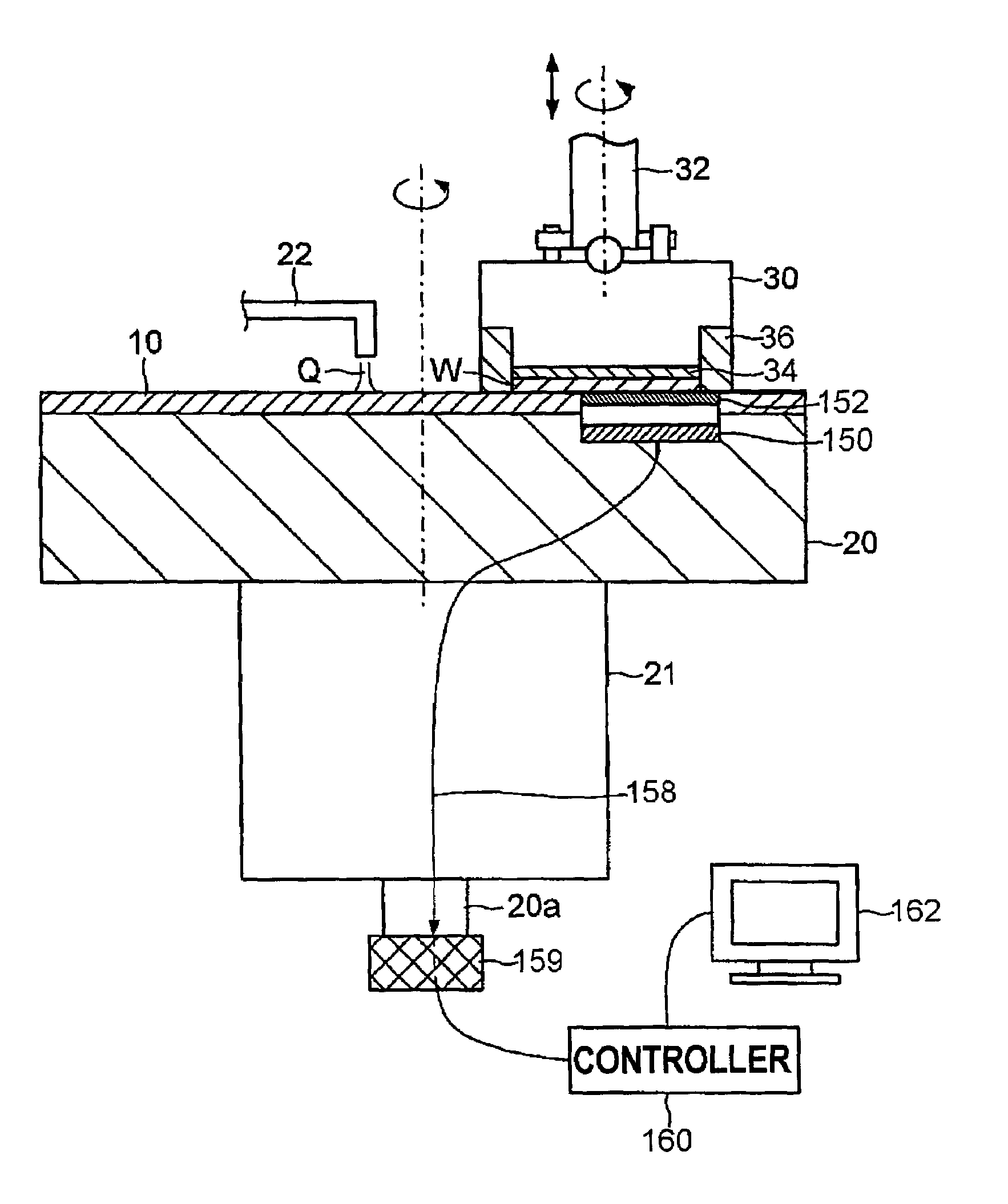
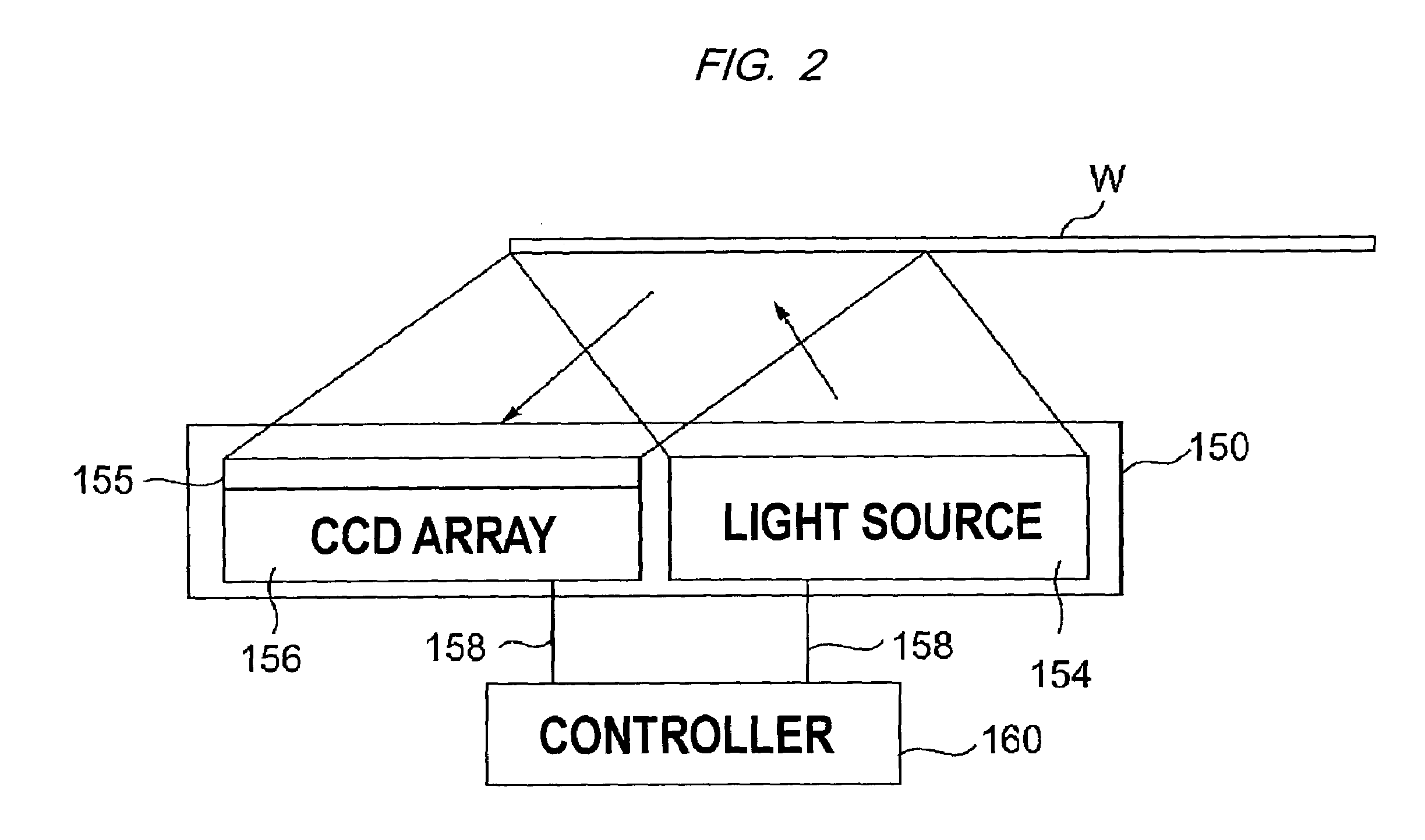
[0028]FIG. 1 is a schematic cross-sectional view showing a polishing apparatus according to the present invention. As shown in FIG. 1, the polishing apparatus has a polishing table 20 having a polishing pad 10 attached on an upper surface thereof, and a top ring 30 for holding and pressing a workpiece such as a semiconductor wafer W against an upper surface of the polishing pad 10. The polishing pad 10 has an upper surface serving as a polishing surface which is brought into sliding contact with the semiconductor wafer W to be polished. The polishing surface may alternatively be formed by an upper surface of a fixed abrasive plate comprising fine abrasive particles made of CeO2 or the like which are fixed by a binder of synthetic resin.

[0029]The polishing table 20 is coupled to a motor 21 disposed below the polishing table 20. Thus, the polishing table 20 is rotatable about its axis as shown by an arrow in FIG. 1. The polishing apparatus has a polishing liquid supply nozzle 22 provi...

second embodiment

[0039]The aforementioned film thickness measuring device may be incorporated into a polishing apparatus for performing electrolytic polishing. FIGS. 4A and 4B are schematic views showing an electrolytic polishing apparatus in which the film thickness measuring device is incorporated. The polishing apparatus according to the present embodiment has a plurality of electrodes 200 disposed in parallel with each other. The electrodes 200 have upper surfaces covered with an ion exchanger (not shown). The electrodes 200 are connected alternately to an anode and a cathode of a power supply (not shown) to form processing electrodes and feeding electrodes, respectively. For example, when copper is to be polished, electrolytic polishing is performed on the cathode. Therefore, electrodes connected to the cathode form processing electrodes, and electrodes connected to the anode form feeding electrodes.

[0040]When the semiconductor wafer W is polished, the semiconductor wafer W is brought into con...


PUM

PropertyMeasurementUnit
thicknessaaaaaaaaaa
wavelengthaaaaaaaaaa
radial lengthsaaaaaaaaaa

Abstract

A polishing apparatus has a polishing table having a polishing surface, a top ring for holding a workpiece to be polished and pressing the workpiece against the polishing surface on the polishing table, and a film thickness measuring device embedded in the polishing table. The film thickness measuring device includes a light source for applying light having a predetermined wavelength to a surface of the workpiece, a spectroscope for separating light reflected from the surface of the workpiece, and a charge coupled device array for capturing light separated by the spectroscope. The polishing apparatus also has a controller operable to analyze information captured by the charge coupled device array over the entire surface of the workpiece to obtain a film thickness at a desired point on the surface of the workpiece.

Description

BACKGROUND OF THE INVENTION[0001]1. Field of the Invention[0002]The present invention relates to a polishing apparatus for polishing a workpiece to be polished, and more particularly to a polishing apparatus having a film thickness measuring device for measuring a film thickness of a surface of a workpiece such as a semiconductor wafer.[0003]2. Description of the Related Art[0004]As semiconductor devices have become more highly integrated in recent years, circuit interconnections have become finer and distances between those circuit interconnections have become smaller. In the case of photolithography, which can form interconnections that are at most 0.5 μm wide, it is required that surfaces on which pattern images are to be focused by a stepper should be as flat as possible because the depth of focus of an optical system is relatively small. A polishing apparatus for performing chemical mechanical polishing (CMP) has been used for planarizing such a semiconductor wafer.[0005]In a c...

Claims


Application Information

Patent Timeline
Patent Type & Authority Patents(United States)
IPC IPC(8): B24B49/00B23H5/08B24B37/013B24B49/02B24B49/12G01B11/06H01L21/304
CPCB23H5/08B24B37/013G01B11/0625B24B49/12B24B37/046
Inventor SHIMIZU, KAZUOOHTA, SHINROTSUKADA, AKIHIRO
Owner EBARA CORP
Why Eureka
Try Eureka