
Locally-distributed electrode and method of fabrication

Inactive Publication Date: 2006-04-04
TELEDYNE SCI & IMAGING
View PDF1 Cites 10 Cited by
  • Summary
  • Abstract
  • Description
  • Claims
  • Application Information

AI Technical Summary

Benefits of technology

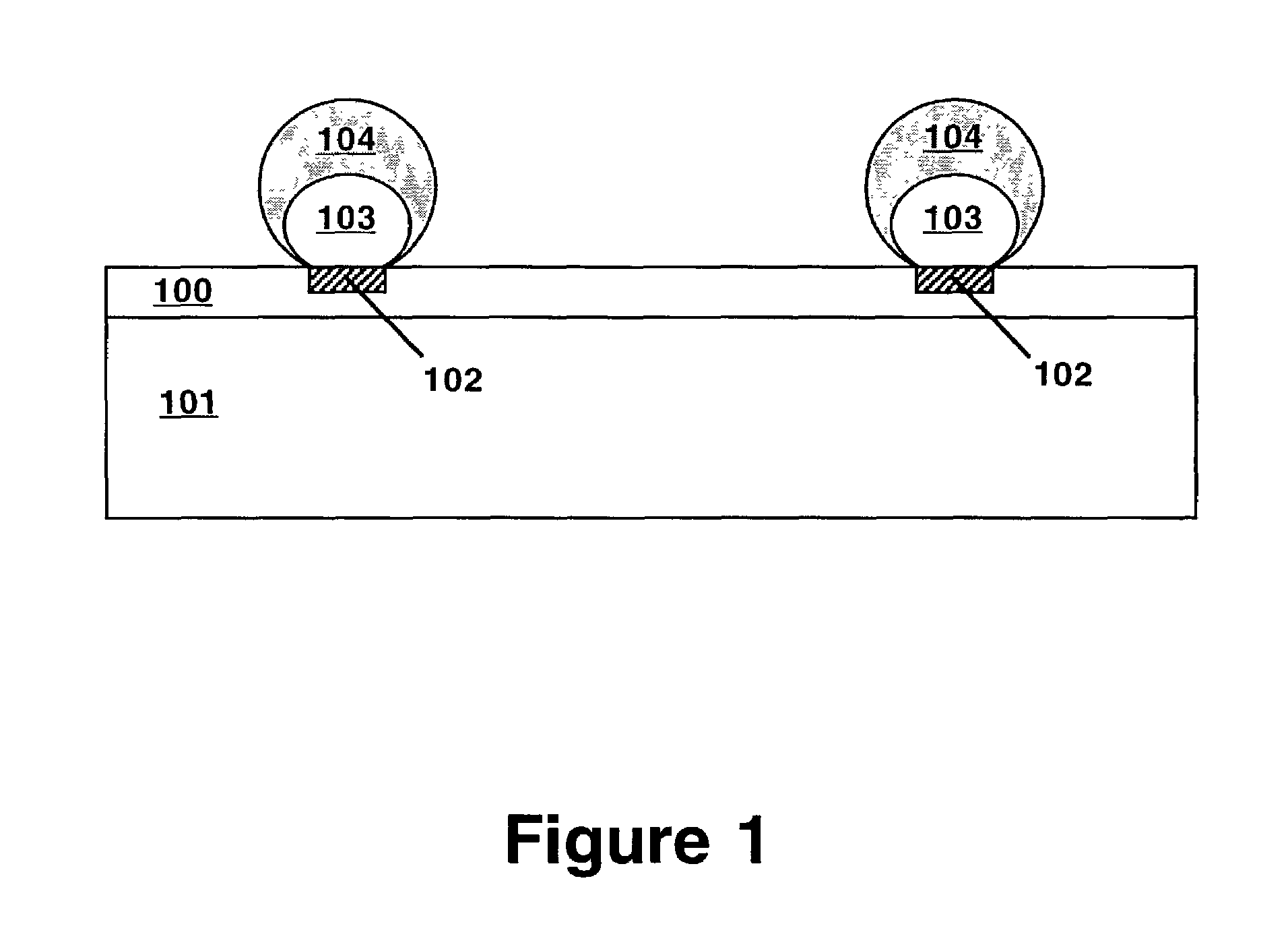
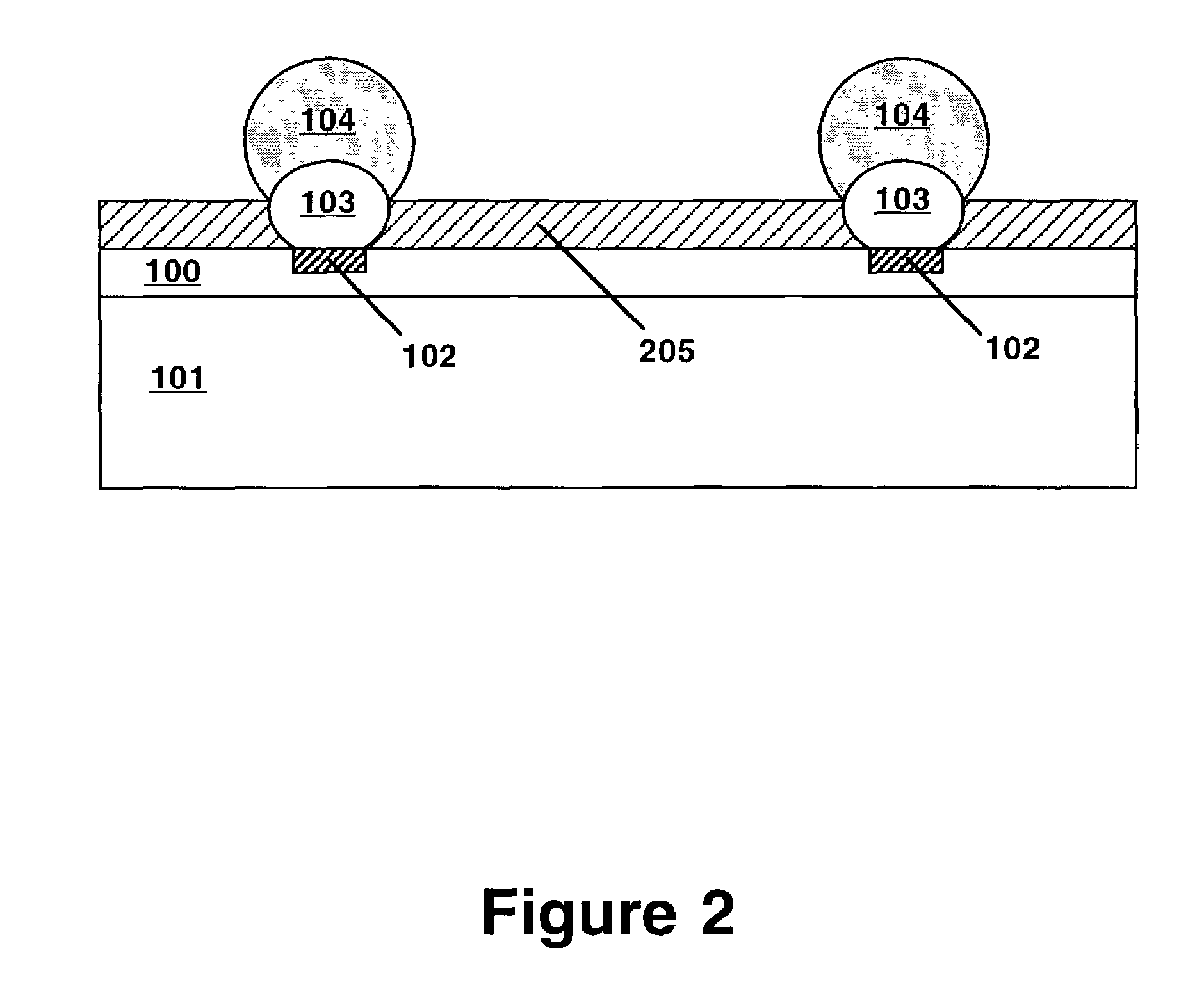
[0012]The noble metal nuclei can be grown into larger islands by continued electrodeposition of the same metal or a different metal (which may be a non-noble metal). The density of noble metal nuclei may be controlled via the preparation conditions for the conducting metallic oxide and by pretreatments that affect the density of defect sites. For example, the defect density may be decreased by annealing the metallic oxide at elevated temperatures and increased by abrading or etching the surface. Additional noble metal nuclei may be electrodeposited via a more negative nucleation pulse (possibly followed by further growth at a less negative potential) or may be deposited by sub-monolayer vacuum evaporation or sputtering (followed by growth via electrodeposition). Heat treatments may be used to improve the adhesion and electrical connection of the noble metal nuclei to the oxide and / or to decrease the reactivity of exposed transparent metallic oxide material. Thin layers of insulating materials may also be used to suppress extraneous reactions on the transparent conducting metallic oxide surface.
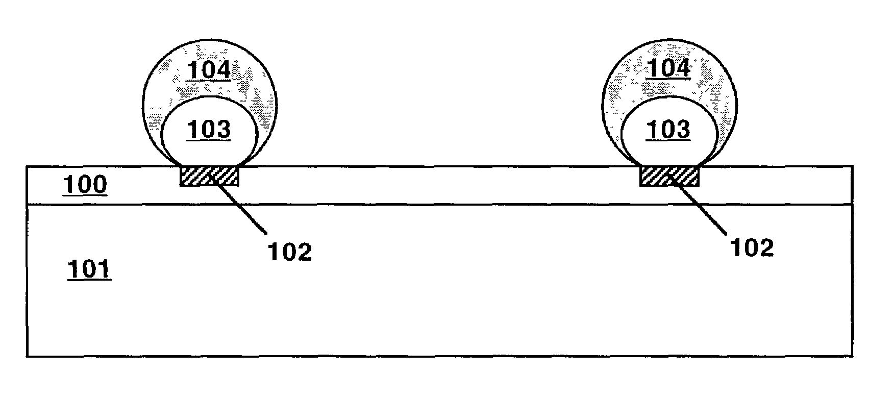
[0013]For REM smart window devices, the dot matrix counter electrode is preferably comprised of microscopic islands of noble metal covered with electrodeposited mirror metal that are distributed uniformly but randomly in a dot matrix over the surface of a continuous layer of transparent conducting metallic oxide. During mirror erasure to increase device transmission, mirror metal electrodeposition occurs preferentially on the metallic islands because of the higher potential required for deposition on the exposed metallic oxide surface, which serves as a current collector. Spherical diffusion of mirror metal ions to such microscopic islands provides much higher current carrying capability (compared to planar diffusion to larger grid lines), and results in nearly spherical electrodeposits. Spherical dot matrix electrodes also have a surface area that is roughly four times the cross-sectional area and thus provide an optimal trade-off between fast mirror switching and high maximum light transmission.
[0014]The method of the present invention is particularly useful for fabricating counter electrodes for REM smart window devices since it avoids the use of expensive photolithography and is readily scalable to large areas. In addition, the three-dimensional microscopic islands of the dot matrix counter electrode have greatly enhanced current carrying capability and, because of their small size and random distribution, are not visible to the naked eye and do not produce interference patterns. This invention could also be used to produce locally distributed electrodes for other applications. For example, electroanalytical sensitivity could be greatly increased by the higher total current for a dot matrix array of nano-scale electrodes compared to a single nano-scale electrode.

Problems solved by technology

However, the electrochromic smart window devices which are known in the prior art have narrow dynamic ranges and involve light absorption in operation, resulting in heat being generated and transferred into the interior space by conduction, convection and infrared radiation.
In addition, electrochromic devices typically utilize a relatively slow ion insertion electrochemical process that limits switching speed and cycle life.
Heating of electrochromic devices by light absorption further reduces the device lifetime.
Other types of smart windows, such as liquid crystal and suspended particle devices, also have limited dynamic range and typically have the added disadvantage of requiring a continuously applied voltage to maintain a given transmissive state.
Commercialization of REM smart window devices has been hindered by the expense and performance of the locally distributed counter electrode, which must present a relatively small cross-sectional area to avoid excessive light blockage that would decrease the maximum transmission of the device.
The photolithographic process is inherently expensive and not readily scalable to large areas.
In addition, fine grid lines (<10 μm wide) are needed so as to be invisible to the eye, but grid lines of such size are prone to damage during the photoresist liftoff process, which further increases the fabrication costs.
Fine grid lines also tend to produce light interference patterns that distort images seen through the window.
Consequently, the current carrying capability for such grids with good light transmission is very low (approximately 5–10% of that for the mirror electrode).

Method used


Image

  • Locally-distributed electrode and method of fabrication
  • Locally-distributed electrode and method of fabrication
  • Locally-distributed electrode and method of fabrication

Examples


example 1

[0030]After being subjected to platinum electrodeposition at 0.40 mA / cm2 to 0.60 C / cm2 of charge, FTO and ITO films were examined by scanning electron microscopy (SEM) and energy dispersive analysis of x-rays (EDAX). The FTO surface had more texture but a relatively uniform distribution of approximately spherical Pt nuclei (about 0.2 μm in diameter) was obtained for both materials. The composition of the Pt nuclei was verified by EDAX analysis. The density of nuclei on the ITO sample was about 3×10⁸ / cm2, which for spherical nuclei of 0.2 μm diameter would block 1% of the light and give a surface area of 4% of the geometric area. The density of the Pt nuclei on the FTO sample was comparable to that for the ITO sample. Adhesion of the Pt nuclei was at least reasonably good since the density remained the same after vigorous water rinsing. These data show that Pt nuclei can be deposited at defect sites on ITO and FTO at a density appropriate for REM counter electrode use. For this nucle...

example 2

[0031]Platinum was electrodeposited on an ITO film at 0.40 mA / cm2 to 5.2 C / cm2 of charge. From SEM / EDAX analysis, Pt islands that appeared to be roughly spherical (about 0.3 μm diameter) were distributed at a density of 2×10⁸ / cm2 uniformly over the ITO surface. The current carrying capability of this Pt dot matrix array was evaluated by cyclic voltammetry (50 mV / s) in a typical REM electrolyte comprised of 1.5 M AgI and 2.0 M LiBr in gamma-butyrolactone (GBL) solvent. A silver film on a platinized ITO substrate was used as a combination counter electrode and reference electrode. Good performance for the Pt dot matrix electrode up to a current of 2.0 mA / cm2 (geometric area) was indicated by Ag electrodeposition current that increased linearly with negative electrode potential and exhibited very little overvoltage and hysteresis, and by anodic current that decreased to a low value after deposited Ag was electrochemically stripped from the electrode. The integrated charges associated w...

example 3

[0032]Platinum was electrodeposited on an ITO film at a constant electrode potential of −0.37 V vs. SCE to 0.80 C / cm2 of charge. SEM / EDAX analysis detected approximately spherical Pt nuclei (about 0.1 μm diameter) at a density of 1×10⁸ / cm2 distributed uniformly over the ITO surface.


PUM

PropertyMeasurementUnit
Temperatureaaaaaaaaaa
Densityaaaaaaaaaa
Currentaaaaaaaaaa

Abstract

A locally distributed electrode is made by placing a conducting metallic oxide layer and a counter electrode in contact with a noble metal electroplating solution and applying a negative potential to the metallic oxide layer relative to the counter electrode, such that the noble metal is electrodeposited from the solution preferentially at defect sites on a surface of the metallic oxide layer. The noble metal nuclei are selectively electrodeposited at the defect sites to form a locally distributed electrode made up of a dot matrix of metallic islands. For reversible electrochemical mirror (REM) devices, the presence of the noble metal renders mirror metal electrodeposition at the defect sites reversible so that the defects become part of the dot matrix electrode and extraneous deposition of the mirror metal on the conducting metallic oxide is avoided. This method avoids the use of expensive photolithography, is readily scalable to large areas, and produces electrodes that offer the optimum compromise between high current carrying capability and high light transmission.

Description

CROSS-REFERENCE TO RELATED APPLICATIONS[0001]This application is related to U.S. Pat. Nos. 5,903,382, 5,923,456, 6,111,685, 6,166,847, 6,256,135, 6,301,039 and 6,400,491, and to U.S. patent application Ser. No. 10 / 066,210, filed Jan. 31, 2002 (entitled “Reversible Electrodeposition Device with Ionic Liquid Electrolyte”), all of which are assigned to the assignee of the present application. The teaching of each of these patents and patent applications is incorporated herein by reference.BACKGROUND OF THE INVENTION[0002]1. Field of the Invention[0003]This invention is concerned with fabrication of locally distributed electrodes that are particularly useful in smart windows for controlling the reflectance and transmission of electromagnetic radiation.[0004]2. Description of the Related Art[0005]Smart windows are designed to reduce the amount of energy consumed for climate control of buildings and transportation vehicles by controlling the amount of solar radiation which is transmitted ...

Claims


Application Information

Patent Timeline
IPC IPC(8): C25B11/00C25D5/02G02F1/1506G02F1/155
CPCC25D5/02G02F1/155G02F1/1506
Inventor TENCH, D. MORGAN
Owner TELEDYNE SCI & IMAGING
Learn More