Method for optimized laser annealing smoothing

a laser annealing and smoothing technology, applied in the field of post-crystallization annealing techniques, can solve the problems of not being able to control all these processes, the inability of conventional methods to achieve such quality differentiation, and the loss of throughput, so as to reduce the diffraction pattern of the mask edg

Inactive Publication Date: 2006-04-18
SHARP KK
View PDF3 Cites 3 Cited by
  • Summary
  • Abstract
  • Description
  • Claims
  • Application Information

AI Technical Summary

Benefits of technology

[0020]The present invention introduces a single-mask that includes sections of 100% light transmission, to melt a semiconductor film, and cross-hatched sub-resolution aperture sections around at least some of the mask edges. In this manner, one mask can be used for both annealing and smoothing. The aperture patterns reduce mask edge diffraction patterns that unintentionally melt the silicon film during the smoothing process.

Problems solved by technology

When forming thin film transistors (TFTs) for use in liquid crystal display (LCD) or other microelectronic circuits, the location of transistors channel regions, the orientation of regular structured polycrystalline silicon (poly-Si) or single-grain-crystalline silicon, and the surface roughness are important issues.
The most important reason for this end result is the inability of conventional methods to achieve such quality differentiation.
In the case of conventional laser annealing, some differentiation is possible, but the price, in terms of loss of throughput, is very high for the modest performance gains realized.
Further, not all these processes can be location controlled.
This kind of non-uniformity is highly detrimental for critical-application TFTs where uniformity of characteristics is more essential than absolute performance.
The drawback to such an approach is that due to volume expansion of the Si material during solidification, a large peak appears in the center of each irradiated region with a magnitude approximately equal to that of the film thickness.
This peak-to-valley roughness can be detrimental to the characteristics of devices subsequently fabricated on the thin film.

Method used


Image

  • Method for optimized laser annealing smoothing
  • Method for optimized laser annealing smoothing
  • Method for optimized laser annealing smoothing

Examples


Embodiment Construction

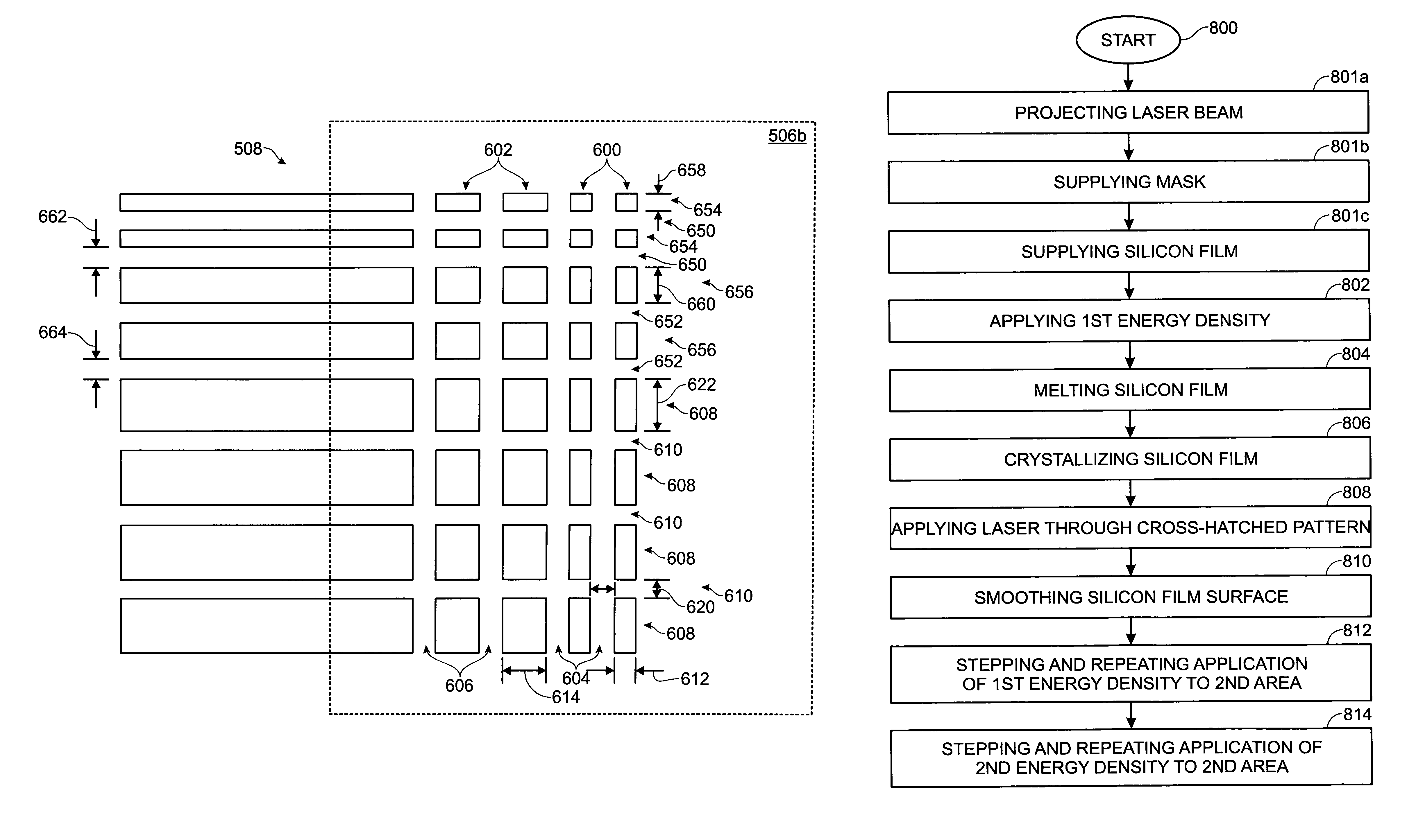
[0032]FIG. 5 is a plan view of the present invention laser annealing mask with cross-hatched sub-resolution aperture patterns. The mask 500 comprises a first section 502 with aperture patterns 504 (an example area is shown in the dotted line box) for transmitting approximately 100% of incident light. The mask 500 also includes at least one section with cross-hatched sub-resolution aperture patterns 506a and / or 506b (as shown in the dotted line boxes) for diffracting incident light. As described below, the mask 500 can include a plurality of sections with cross-hatched sub-resolution aperture patterns.

[0033]Shown is a second mask section 508 with cross-hatched sub-resolution aperture patterns 506a in an area adjacent a leading mask vertical edge 510 with respect to a first direction 512. That is, edge 510 is the leading edge when the mask 500 is moved in the first direction 512. A third mask section 514 with cross-hatched sub-resolution aperture patterns 506 is an area adjacent a tra...


PUM

PropertyMeasurementUnit
widthaaaaaaaaaa
widthaaaaaaaaaa
vertical gap widthaaaaaaaaaa

Abstract

A laser annealing mask is provided with cross-hatched sub-resolution aperture patterns. The mask comprises a first section with aperture patterns for transmitting approximately 100% of incident light, and at least one section with cross-hatched sub-resolution aperture patterns for diffracting incident light. In one aspect, a second mask section with cross-hatched sub-resolution aperture patterns has an area adjacent a vertical edge and a third mask section with cross-hatched sub-resolution aperture patterns adjacent the opposite vertical edge, with the first mask section being located between the second and third mask sections. The section with cross-hatched sub-resolution aperture patterns transmits approximately 40% to 70%, and preferably 50% to 60% of incident light energy density. In some aspects, the section with cross-hatched sub-resolution aperture patterns includes a plurality of different cross-hatched aperture patterns. The cross-hatched sub-resolution aperture patterns can be defined by horizontal gap and slits, as well as vertical gap and slits.

Description

RELATED APPLICATIONS[0001]This application is a divisional of application Ser. No. 10 / 232,089, filed Aug. 29, 2002, now U.S. Pat. No. 6,777,276 entitled “System and Method for Optimized Laser Annealing Smoothing Mask,” invented by Crowder et al., which is a continuation-in-part of application Ser. No. 10 / 124,826, filed Apr. 17, 2002, entitled, Laser Annealing Mask and Method for Smoothing an Annealed Surface, invented by Mitani et al.BACKGROUND OF THE INVENTION[0002]1. Field of the Invention[0003]This invention generally relates to integrated circuit (IC) thin film processing techniques and, more particularly, to post-crystallization annealing techniques that can be applied to semiconductor or metal films at low temperatures.[0004]2. Description of the Related Art[0005]When forming thin film transistors (TFTs) for use in liquid crystal display (LCD) or other microelectronic circuits, the location of transistors channel regions, the orientation of regular structured polycrystalline s...

Claims


Application Information

Patent Timeline
Patent Type & Authority Patents(United States)
IPC IPC(8): H01L21/3205B23K26/06H01L21/00H01L21/20H01L21/302H01L21/44H01L21/461H01L21/84
CPCH01L21/2026B23K26/0656B23K26/066H01L21/02532H01L21/0268
Inventor CROWDER, MARK ALBERTMITANI, YASUHIROVOUTSAS, APOSTOLOS T.
Owner SHARP KK
Why Eureka
Try Eureka