Single transistor rare earth manganite ferroelectric nonvolatile memory cell

a single transistor, ferroelectric technology, applied in the direction of digital storage, capacitors, instruments, etc., can solve the problems of not being able to switch ferroelectric materials, not being able to operate devices at low voltages, and most of the voltage will drop over the interfacial layer, so as to prevent any early evaporation problems, good step coverage, excellent uniformity and composition control

Inactive Publication Date: 2006-04-18
COVA TECH
View PDF101 Cites 45 Cited by
  • Summary
  • Abstract
  • Description
  • Claims
  • Application Information

AI Technical Summary

Benefits of technology

[0019]The ferroelectric materials of the present invention are deposited preferably by metallorganic chemical vapor deposition techniques (MOCVD), although other methods such as PECVD or MOD could be used. The MOCVD process preferably uses a liquid source delivery and flash evaporation method, since the precursors preferably used typically have low vapor pressure, making other methods such as vapor delivery with bubblers difficult. Examples of precursors used for CeMnO3, a special embodiment of the current invention, are Cerium (IV) tris-tetram...

Problems solved by technology

If the capacitance of the interfacial layer is much smaller than the capacitance of the ferroelectric layer, most of the voltage will drop over t...

Method used


Image

  • Single transistor rare earth manganite ferroelectric nonvolatile memory cell
  • Single transistor rare earth manganite ferroelectric nonvolatile memory cell
  • Single transistor rare earth manganite ferroelectric nonvolatile memory cell

Examples


Embodiment Construction

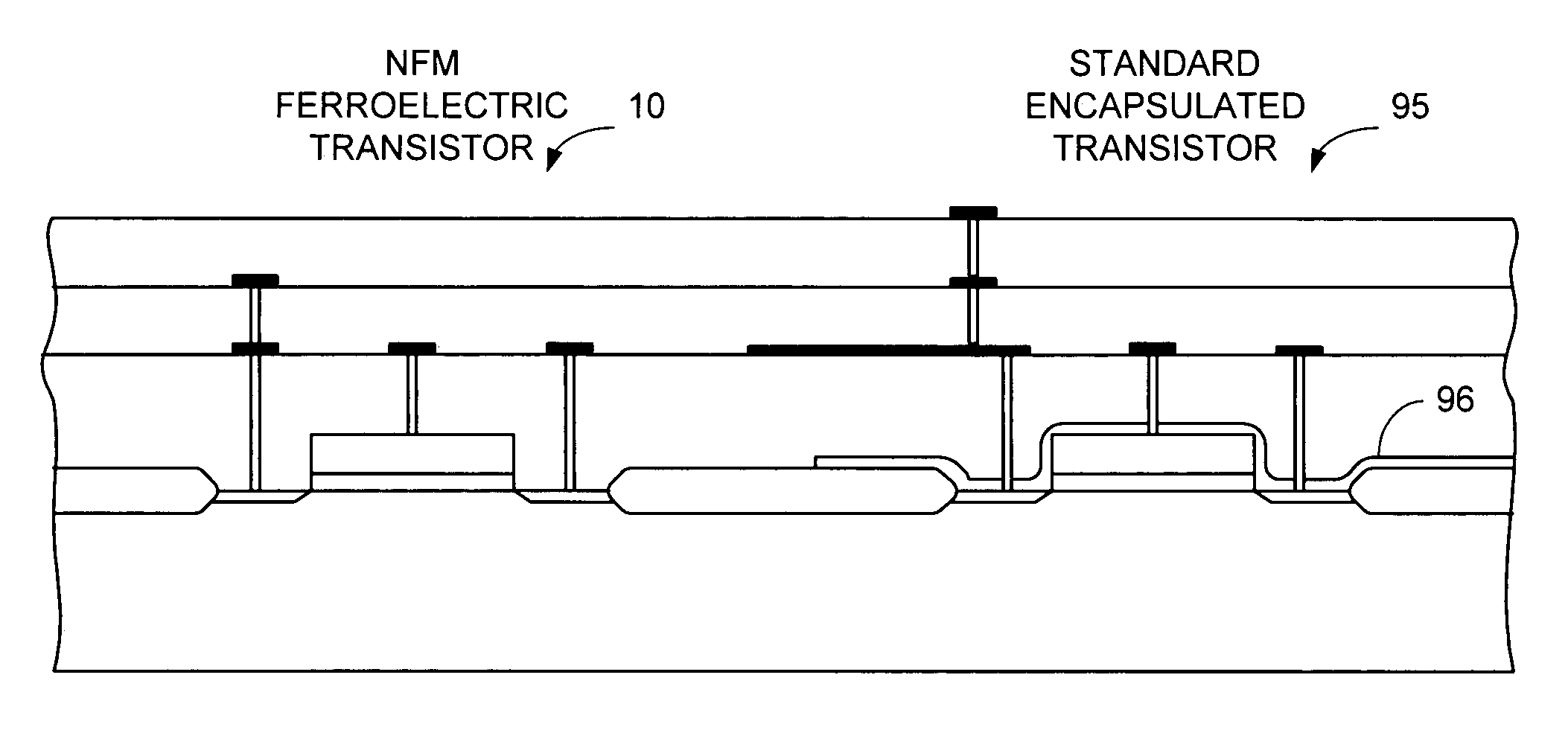
[0031]A description of a 1 transistor (1T) memory cell 10 in accordance with the present invention is shown in FIG. 2a. The 1T memory cell 10 consists of a substrate 20 of a suitable material such as silicon. Substrate 20 may be the starting material for a complex integrated circuit. Shown in FIG. 2a is only the memory cell itself. The cell may be the building block of a memory array that in turn is interconnected with peripheral circuitry such as decoders, sense amplifiers and input / output circuitry (not shown). A ferroelectric thin film layer 30 is deposited directly onto substrate 20. An interfacial layer 31 is formed between substrate 20 and ferroelectric layer 30 either automatically during deposition of ferroelectric layer 30 or deliberately as a separate processing step prior to deposition of ferroelectric layer 30. The ferroelectric layer 30 is deposited as described below and the interfacial layer is a mixture of the oxides of silicon and the rare earth.

[0032]The ferroelect...


PUM


Abstract

A memory device is formed of the one transistor cell type. Such a device has a substrate, a ferroelectric layer which is a film of rare earth manganite, and an interfacial oxide layer being positioned between the substrate and the ferroelectric layer. The invention includes such a device and methods of making the same.

Description

[0001]This applications is a 371 of PCT / US02 / 13095 filed Aug. 24, 2001, which claims benefit of provisional 60 / 227,858 filed Aug. 24, 2000 And claims benefit of provisional 60 / 272,986 filed Mar. 2, 2001.FIELD OF THE INVENTION[0002]The present invention relates to the field of nonvolatile memory devices using a single transistor as the only element in the memory cell and the formation of this transistor with a rare earth manganite thin film ferroelectric material as the gate dielectric.BACKGROUND OF THE INVENTION[0003]Nonvolatile ferroelectric random access memory (FeRAM) devices represent an emerging, multibillion-dollar market. The most advanced FeRAMs utilize a 1-transistor / 1 capacitor (1T1C) cell technology and a destructive read out (DRO) scheme. These devices compete with EEPROMs, battery backed static RAMs (BBSRAMs), and Flash nonvolatile memory devices.[0004]FeRAM is a type of semiconductor memory, constructed similarly to a Dynamic Random Access Memory (DRAM), but which stor...

Claims


Application Information

Patent Timeline
IPC IPC(8): H01L29/792G11C11/22H01L21/02H01L21/28H01L21/8246H01L21/8247H01L27/105H01L27/115H01L29/51H01L29/78H01L29/788
CPCG11C11/22H01L21/28291H01L27/105H01L29/78391H01L27/11509H01L29/516H01L27/11502H01L28/56H01L29/40111H10B53/00H10B53/40H10B69/00
Inventor GNADINGER, FRED P.
Owner COVA TECH
Why Eureka
Try Eureka