Tilted cavity semiconductor laser (TCSL) and method of making same

a semiconductor laser and tilting cavity technology, applied in the direction of lasers, laser optical resonator construction, laser construction details, etc., can solve the problem of unsatisfactory temperature dependence of the wavelength of emitted light, approach that requires very complicated technological steps, and drastically reduces the number of possible materials for bragg mirrors

Inactive Publication Date: 2006-04-18
INNOLUME
View PDF12 Cites 21 Cited by
  • Summary
  • Abstract
  • Description
  • Claims
  • Application Information

AI Technical Summary

Benefits of technology

[0009]A novel class of semiconductor lasers, or “tilted cavity lasers” includes at least one active element with an active region generating an optical gain by injection of a current and mirrors. The active element is placed into a cavity. The cavity is designed such that the optical path of the resonant optical mode is tilted with respect to both the vertical direction and the lateral plane. Thus, the feedback both in the vertical and in the lateral direction is provided for the resonant optical mode. Depending on the particular embodiment, the laser operates as both a surface emitting laser and an edge-emitting laser. Employing a tilted optical mode allows the use of substantially fewer layers in the bottom and the top interference reflectors than in conventional lasers. This preserves the necessary high reflection coefficients. Also, a wavelength-stabilized laser is realized for edge-emitters. The wavelength stabilization is due to the difference in the dispersion laws for the tilted optical modes in layers having different refractive indices.

Problems solved by technology

One of the major problems with semiconductor lasers is a variation of the energy band gap with temperature resulting in an undesirable temperature dependence of the wavelength of emitted light, particularly for high output power operation.
However, this approach requires very complicated technological steps as compared to the epitaxial growth of a conventional laser.
This requirement drastically reduces the number of possible materials to be used in Bragg mirrors.
A major disadvantage of the conventional Bragg-stack mirror configuration is that between 40 to over 200 high quality layers may be required to fabricate a complete VCSEL.
A serious disadvantage of this design is unavoidable lithographical steps in fabricating one or two gratings with a lateral periodicity, which do not allow fabricating a laser in a single epitaxial process.
Moreover, in the practically more acceptable situation where only one top grating is used, the bottom Bragg reflector still has all of the limitations and disadvantages characteristic of a conventional VCSEL.

Method used


Image

  • Tilted cavity semiconductor laser (TCSL) and method of making same
  • Tilted cavity semiconductor laser (TCSL) and method of making same
  • Tilted cavity semiconductor laser (TCSL) and method of making same

Examples


Embodiment Construction

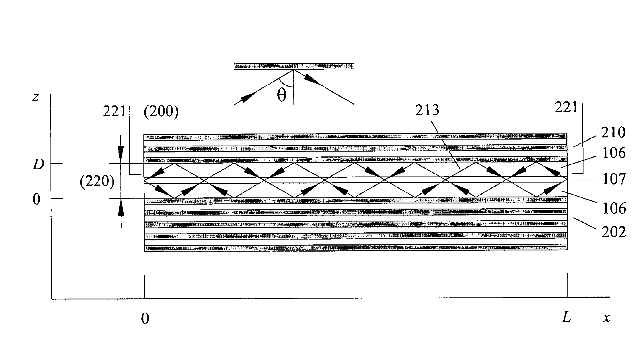
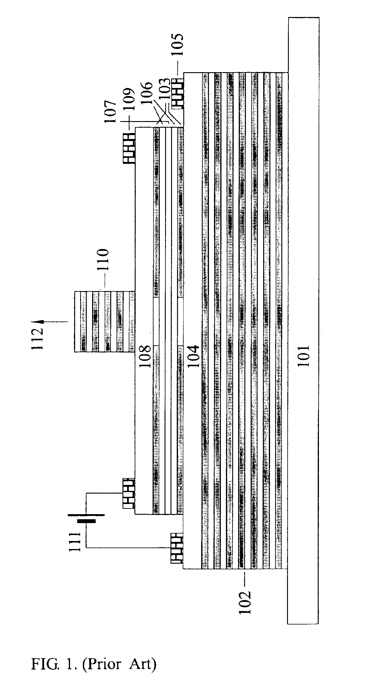
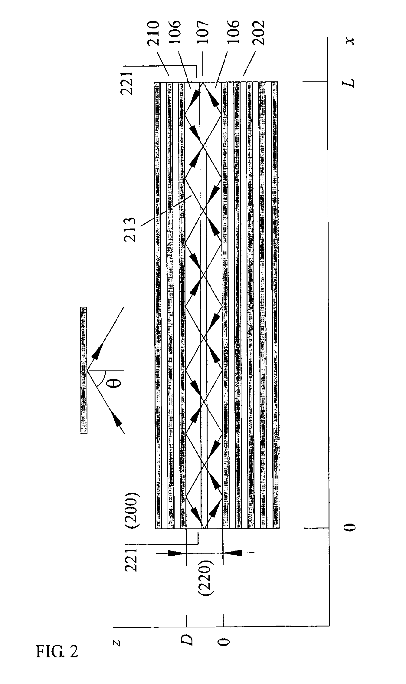
[0042]A prior art surface emitting laser, or more specifically, a vertical cavity surface emitting laser (VCSEL), is shown in FIG. 1. In a surface emitting laser, an active region is generally put into a cavity. An undoped or weakly doped active region is surrounded by n- and p-contact layers, which are generally surrounded by mirrors. The structure is grown epitaxially on a substrate (10). Bragg reflectors are used for the bottom mirror (102). The rest of the VCSEL is an active element.

[0043]A current aperture (13) separates an n-doped current spreading layer (14) having a first metal contact (15), from the weakly doped confinement layers (16) surrounding the active region (17). A second current aperture (13) separates the weakly doped confinement layer (16) from a p-doped current spreading layer (18) having a second metal contact (19). The n-doped current spreading layer (14) sits directly on top of the bottom mirror (102). The active element operates under forward bias (11). The ...


PUM

PropertyMeasurementUnit
reflectivityaaaaaaaaaa
angleaaaaaaaaaa
wavelengthaaaaaaaaaa

Abstract

A novel class of semiconductor lasers, or “tilted cavity lasers” includes at least one active element with an active region generating an optical gain by injection of a current and mirrors. The active element is placed into a cavity. The cavity is designed such that the optical path of the resonant optical mode is tilted with respect to both the vertical direction and the lateral plane. Thus, the feedback both in the vertical and in the lateral direction is provided for the resonant optical mode. Depending on the particular embodiment, the laser operates as both a surface emitting laser and an edge-emitting laser. Employing a tilted optical mode allows the use of substantially fewer layers in the bottom and the top interference reflectors than in conventional lasers. This preserves the necessary high reflection coefficients. Also, a wavelength-stabilized laser is realized for edge-emitters. The wavelength stabilization is due to the difference in the dispersion laws for the tilted optical modes in layers having different refractive indices.

Description

BACKGROUND OF THE INVENTION[0001]1. Field of the Invention[0002]The invention pertains to the field of semiconductor devices. More particularly, the invention pertains to surface emitting lasers and wavelength-stabilized edge-emitting lasers.[0003]2. Description of Related Art[0004]The semiconductor laser plays an important role in optical fiber transmission and signal amplification systems, wavelength division multiplexing transmission systems, wavelength division switching systems, and wavelength cross-connection systems, as well as in the field of optical measurements.[0005]One of the major problems with semiconductor lasers is a variation of the energy band gap with temperature resulting in an undesirable temperature dependence of the wavelength of emitted light, particularly for high output power operation. One approach to wavelength stabilization includes using a distributed-feedback laser. Some examples of this approach include U.S. Pat. No. 3,760,292, entitled “INTEGRATED FE...

Claims


Application Information

Patent Timeline
Patent Type & Authority Patents(United States)
IPC IPC(8): H01S5/00G02F1/017H01S1/00H01S5/10H01S5/18H01S5/183H01S5/20H01S5/50
CPCH01S5/18341H01S5/0028H01S5/0265H01S5/18302H01S5/18327H01S5/50H01S5/18391H01S5/2027H01S5/426H01S5/187
Inventor LEDENTSOV, NIKOLAISHCHUKIN, VITALY
Owner INNOLUME
Why Eureka
Try Eureka