Method for fabricating a probe pin for testing electrical characteristics of an apparatus

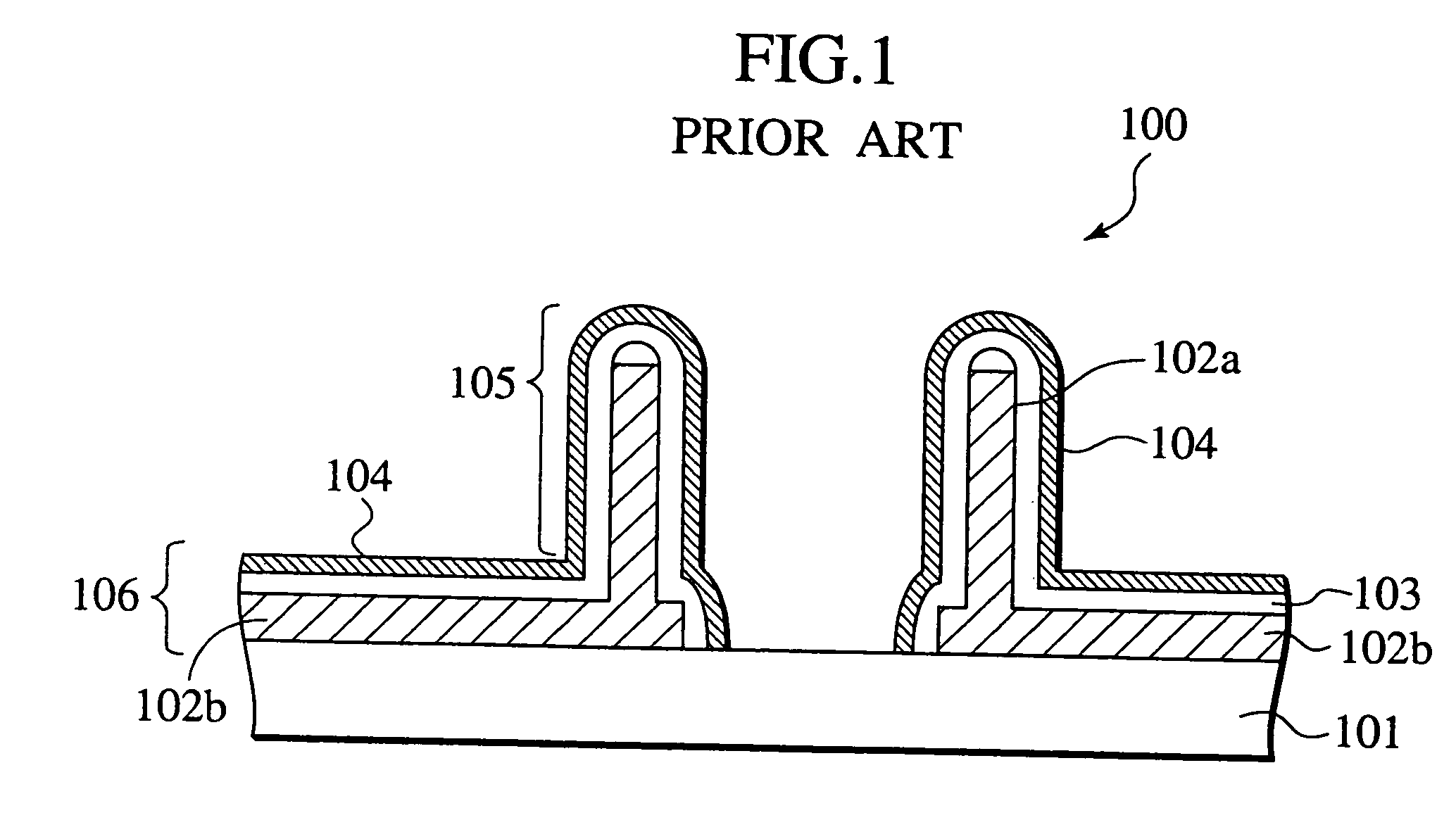
a technology of electrical characteristics and probe pins, which is applied in the direction of testing/measurement of semiconductor/solid-state devices, coupling device connections, instruments, etc., can solve the problems of limiting the freedom of two-dimensional layout of probes, affecting the quality of electrical characteristics of electrical components, and inevitably long wiring lengths. , to achieve the effect of eliminating signal transfer variation, reducing contact resistance, and high density

Inactive Publication Date: 2006-04-25
KK TOSHIBA
View PDF29 Cites 110 Cited by
  • Summary
  • Abstract
  • Description
  • Claims
  • Application Information

AI Technical Summary

Benefits of technology

[0012]It is another object of the invention to provide a probe assembly, which is a combination of a probe pin and an electrode connected to the base of the test probe. This probe assembly allows the pitch of probe pins to be reduced when a number of pins are arranged on a board, and the lengths of the leads from the probes can be made almost equal. The probe assembly has a low contact-resistance, and is suitable to measurement at a high frequency.
[0015]To achieve the objects, a probe pin for testing electric characteristics of an apparatus comprises a silicon pin core, and a conductive layer covering the entire surface of the silicon pin core. In this text, “covering the entire surface” means that not only the tip or the side face of the silicon pin, which is brought into direct contact with an integrated circuit to be tested, but also the bottom face of the silicon pin core is coated with the conductive layer. By coating the bottom face of the silicon pin, the bottom face of the silicon pin is connected directly to the electrode placed in the print wiring board, which is further connected to a tester. The direct connection between the bottom face of the silicon pin and the electrode eliminates the necessity of leads extending from the side face of the associated silicon pins in a two-dimensional plane. Consequently, the density of the silicon pins is greatly increased when multiple pins are arranged on a wiring board.
[0020]In still another aspect of the invention, a probe card is provided. The probe card comprises one or more probe pins and a print wiring board having one or more electrode, each electrode being positioned below an associated probe pin, and connected to the bottom of the associated probe pin. Each probe pin comprises a silicon pin core and a conductive layer covering the entire surface of the silicon pin core. Because each probe pin is connected directly to the electrode at its bottom without requiring leads, the probe card has a fine-pitch and high-dense structure. This probe card can also eliminates variation in signal transfer due to differences in the lengths of the leads extracted from the associated pins. Accordingly, the probe card can measure a high-frequency signal in a stable manner. Since the lead or the extracted electrode, which was required in the conventional test probe, is eliminated, the contact resistance is greatly reduced, and highly precise measurement can be realized.

Problems solved by technology

However, the conventional silicon probe requires a certain space around each pin in order to extract and arrange the lead on the substrate.
These factors greatly limit the freedom of producing two-dimensional layout of a probe, especially with respects to the positions and the density of the probe pins.
This limitation is a fatal obstacle to producing a fine-pitch probe for testing a highly dense circuit.
Another problem in the conventional probe set is that if the leads from the associated probes are arranged in the two-dimensional manner, the wiring length becomes inevitably long, and in addition, the lengths of the leads extending from different probes differ from one another.
The long lead causes the contact resistance to increase between the probe pin and the electrode formed on the substrate, which results in a measurement error.

Method used


Image

  • Method for fabricating a probe pin for testing electrical characteristics of an apparatus
  • Method for fabricating a probe pin for testing electrical characteristics of an apparatus
  • Method for fabricating a probe pin for testing electrical characteristics of an apparatus

Examples


first embodiment

(First Embodiment)

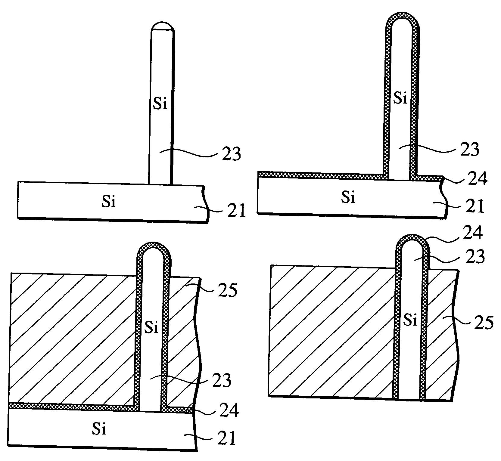
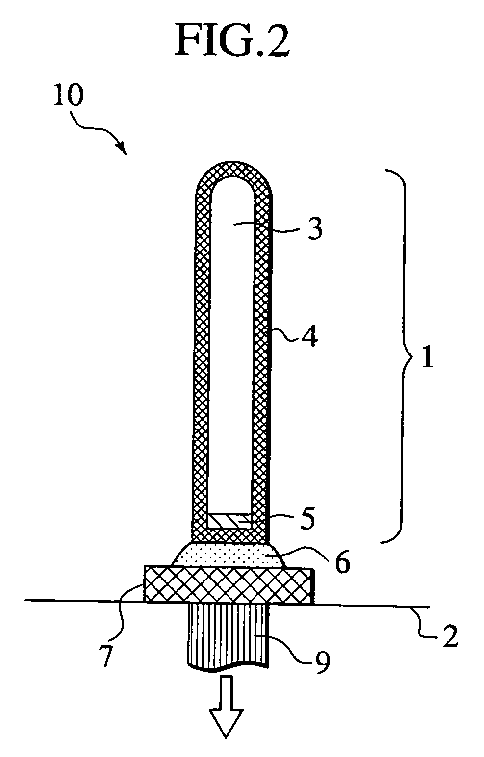
[0034]FIG. 2 illustrates a probe assembly 10 which includes a probe pin 1 for testing electric characteristics of, for example, a semiconductor device, and an electrode 7 connected directly to the bottom of the probe pin 1. The probe pin 1 comprises a single crystal silicon pin core 3, and a gold (Au) film 4 covering the entire surface of the silicon pin core 3. The probe pin 1 also has a nickel silicide (Ni2Si) film 5 at the bottom of the silicon pin core 3. Because the resistance of silicon is comparatively high, the tip and the side face (collectively referred to as “the first surface”) of a silicon pine, which are brought into contact with a semiconductor wafer during a test or measurement, were conventionally coated with a low-resistance metal film. The feature of the probe pin 1 is that the bottom (referred to as the “second surface”) of the silicon pin core 3 is also coated with a low-resistance film, for example, a gold (Au) film 4.

[0035]The bottom (i.e., t...

second embodiment

(Second Embodiment)

[0054]FIG. 5 illustrates a probe assembly 30 that includes a probe pin 31 for testing electric characteristics of, for example, a semiconductor integrated circuit, and an electrode 37 connected directly to the bottom of the probe pin by soldering. The probe pin 31 comprises a single crystal silicon pin core 33 and a gold film 34 covering the entire surface of the silicon pin core 33. Unlike the probe pin 1 of the first embodiment, the probe pin 31 does not have a nickel silicide (Ni2Si) film at the bottom. Accordingly, the second face (i.e., the bottom face) of the silicon pin core is directly coated with the gold film 34. The bottom of the electrode 37 is connected to the interconnection 39 extending inside the substrate 32, as in the first embodiment explained in conjunction with FIG. 2. The probe pin 31 is electrically connected to an external circuit via the electrode37 and the interconnection 39.

[0055]FIG. 6 illustrates a process of fabricating the probe pin ...


PUM

PropertyMeasurementUnit
heightaaaaaaaaaa
thicknessaaaaaaaaaa
temperatureaaaaaaaaaa

Abstract

A probe pin for testing electric characteristics of a semiconductor device comprises a silicon pin core (3, 23, 33), and a conductive film (4, 24, 34) covering the entire surface, including the bottom face, of the pin core. The bottom face of the probe pin is connected directly to an electrode (7, 37) positioned in or on a print wiring board. A number of probe pins can be connected to the associated electrodes at a high density, thereby forming a fine-pitch probe card having a superior high-frequency signal characteristic.

Description

RELATED APPLICATIONS[0001]This application is a divisional application of U.S. patent application Ser. No. 09 / 733,228, filed Dec. 8, 2000, now U.S. Pat. No. 6,724,208.[0002]The present patent application claims the benefit of earlier Japanese Patent Application No. 11-363317 filed Dec. 21, 1999, the disclosure of which is entirely incorporated herein by reference.BACKGROUND OF THE INVENTION[0003]1. Field of the Invention[0004]The present invention relates to a probe pin for testing electric characteristics of an apparatus, such as a semiconductor integrated circuit, an LCD, a magnetic recording device, or the like, and to a method for fabricating the probe pin. The invention also relates to a probe card using a set of probe pins.[0005]2. Description of the Related Art[0006]A test probe or a probe card is generally used to test the electric characteristics of a semiconductor integrated circuit printed on a wafer before the wafer is cut into chips. As the pattern of a semiconductor in...

Claims


Application Information

Patent Timeline
Patent Type & Authority Patents(United States)
IPC IPC(8): H05K3/10B81C1/00G01R1/067G01R3/00H01L21/66
CPCG01R1/06761G01R3/00Y10T29/49155Y10T29/49117Y10T29/49147
Inventor MATSUNAGA, NORIAKISHIBATA, HIDEKIHAYASAKA, NOBUO
Owner KK TOSHIBA
Why Eureka
Try Eureka