Electron-emitting device, electron source and image-forming apparatus, and method for manufacturing electron emitting device

a technology of electron emitting device and electron source, which is applied in the manufacture of electric discharge tube/lamp, discharge tube luminescnet screen, discharge tube/light tube, etc., can solve the problems of large driving device, large capacitance power consumption, and high driving voltage of several tens volts, and achieves stable electrical connection, simple process, and excellent characteristics.

Inactive Publication Date: 2006-04-25
CANON KK
View PDF136 Cites 21 Cited by
  • Summary
  • Abstract
  • Description
  • Claims
  • Application Information

AI Technical Summary

Benefits of technology

[0018]The present invention is devised to solve the above problems. The object is to provide an electron-emitting device, an electron source, an image-forming apparatus, and a scheme of manufacturing an electron-emitting device that can reduce an device capacity and a driving voltage, improve the electron emission efficiency, and obtain a high-resolution beam.
[0024]According to the present invention, fiber comprising carbon as a main ingredient is provided on the layer containing a material having growth selectivity. Thus, the fiber comprising carbon as a main ingredient can obtain stable electrical connection and an electron-emitting device having excellent characteristics can be formed with a simple process.

Problems solved by technology

Further, the spint type has a high driving voltage of several tens volts and a capacitive power consumption is large.
Although the horizontal FE can reduce a capacity of an element, a voltage of several hundreds of volts is required for driving because of a large distance between the emitter and the gate, resulting in a large driving device.
Although beam focusing means may be provided on the spint-type and lateral FE electron-emitting device, problems arise such as a complicated manufacturing scheme, an increased device area, and a reduced electron-emission efficiency.

Method used


Image

  • Electron-emitting device, electron source and image-forming apparatus, and method for manufacturing electron emitting device
  • Electron-emitting device, electron source and image-forming apparatus, and method for manufacturing electron emitting device
  • Electron-emitting device, electron source and image-forming apparatus, and method for manufacturing electron emitting device

Examples


example 1

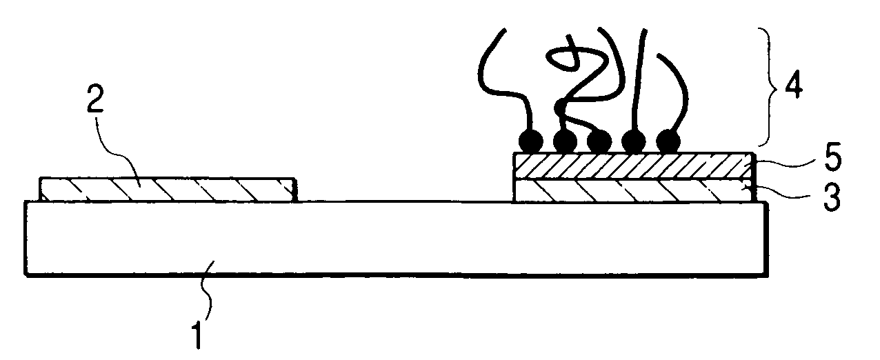
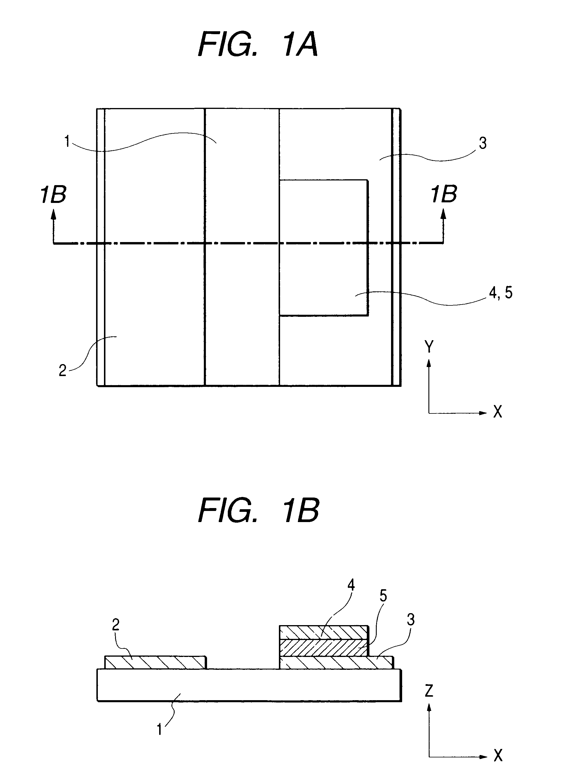
[0129]FIG. 1A is a schematic diagram taken from the top of an electron-emitting device according to Example 1 of the present invention. FIG. 1B is a section view taken along line 1B—1B shown in FIG. 1A.

[0130]In FIGS. 1A and 1B, reference numeral 1 denotes an insulating substrate, reference numeral 2 denotes a extracting electrode, reference numeral 3 denotes a cathode electrode, reference numeral 4 denotes an electron-emitting member, and reference numeral 5 denotes a layer where fibrous carbon is grown.

[0131]Referring to FIGS. 5A to 5E, the following will discuss the detail of a manufacturing process of the electron-emitting device of this example.

(Step 1)

[0132]A quartz substrate is used as the substrate 1. After sufficient cleaning, Ti (not shown) having a thickness of 5 nm and Pt having a thickness of 30 nm are evaporated continuously.

[0133]Next, in a photolithography process, a resist pattern is formed using a positive photoresist (AZ1500 / manufactured by Clariant International L...

example 2

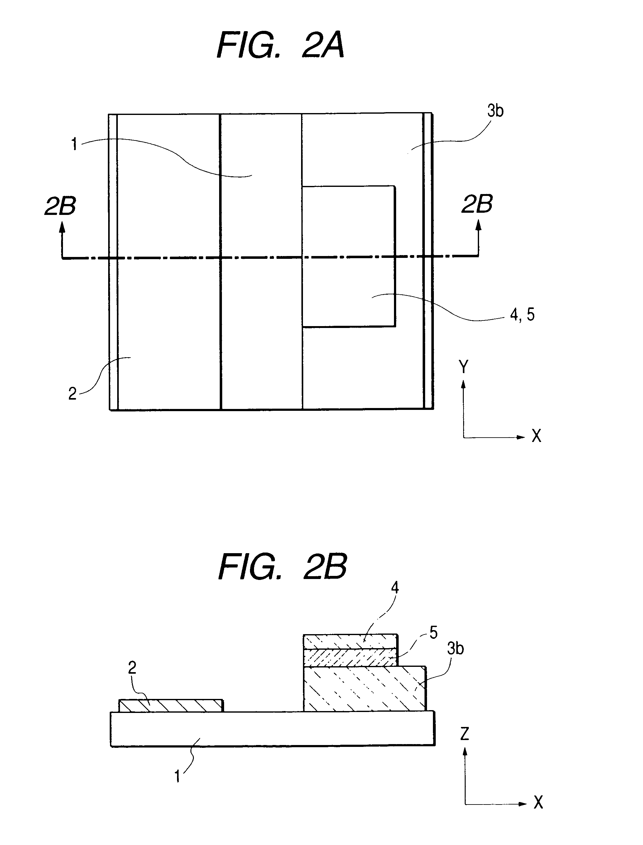
[0158]FIGS. 2A and 2B show Example 2.

[0159]In the present example, an electron-emitting device was manufactured in the same manner as Example 1 except that the cathode electrode 3b was 500 nm in thickness and the extracting electrode 2 was 30 nm in thickness, and measurement was made on If and Ie.

[0160]Other configurations and effects are the same as those of Example 1. Hence, the same members will be indicated by the same reference numerals and the description thereof is omitted.

[0161]In the device configuration of the present example, a position for emitting electrons was positively set at a high position (anode side) from the extracting electrode 2 by increasing a thickness of the cathode electrode 3b.

[0162]With this configuration, since trajectories of electrodes colliding with the gate were reduced, it was possible to prevent a reduction in efficiency and an increase in beam diameter.

[0163]Consequently, in the present device configuration as well, an electron emission current ...

example 3

[0165]FIGS. 3A and 3B show Example 3.

[0166]In the above example, the layer 5 and the electron-emitting member 4 are formed on the cathode electrode 3. In the present example, a layer 5c and an electron-emitting member 4c are formed across the cathode electrode 3 and a gap (space) between the cathode electrode 3 and the gate electrode 2.

[0167]In the step 2 of Example 1, a resist pattern is formed in the same step as Example 1 except that a position for forming a resist pattern is changed. Thus, the description thereof is omitted.

[0168]Besides, in the present example, the layer 5c and the electron-emitting member 4c are extended to an about intermediate point (about a half of a distance between the gaps) of a gap between the cathode electrode 3 and the gate electrode 2 such that a distance is small between the electron-emitting member 4c and a extracting electrode 2.

[0169]This device has an electric field about twice as large as that of the device of Example 1 since its distance betwe...


PUM


Abstract

To provide an electron-emitting device, an electron source, an image-forming apparatus, and a method for manufacturing the electron-emitting device whereby it is possible to reduce a device capacity and a driving voltage, to improve the efficiency of emitting electrons, and to obtain high-resolution beam. The extracting electrode and the cathode electrode are provided on an insulating substrate, a layer having growth selectivity of fibrous carbon is formed on the cathode electrode, and the fibrous carbon is grown via catalyst particles formed on the layer.

Description

BACKGROUND OF THE INVENTION[0001]1. Field of the Invention[0002]The present invention relates to an electron-emitting device, an electron source having the electron emitting device, and an image-forming apparatus for using and applying the electron source, and to a display apparatus for broadcast on television, a display apparatus for a TV conference system, a computer, and so on, and an image-forming apparatus used as an optical printer, which is composed of a photosensitive drum and the like. The present invention further relates to a method for manufacturing an electron-emitting device.[0003]2. Related Background Art[0004]Development of an image-forming apparatus using an electron-emitting device has been pursued in recent years.[0005]A field emission (FE type) electron-emitting device has become a focus of attention as one of cold electron sources. The field emission electron-emitting device applies a strong electric field of 106 V / cm or more on metal and emits an electron from ...

Claims


Application Information

Patent Timeline
Patent Type & Authority Patents(United States)
IPC IPC(8): H01J1/304H01J9/02H01J29/04H01J31/12
CPCB82Y10/00H01J1/304H01J31/127H01J29/86H01J2329/8615H01J2201/30469
Inventor TSUKAMOTO, TAKEO
Owner CANON KK
Why Eureka
Try Eureka