Coupling device using buried capacitors in multilayered substrate

a capacitor and multi-layer substrate technology, applied in semiconductor devices, semiconductor/solid-state device details, waveguides, etc., can solve the problems of compromising the circuit area, affecting the performance of the coupler, and requiring a large area of occupation

Inactive Publication Date: 2006-04-25
NOKIA CORP
View PDF6 Cites 27 Cited by
  • Summary
  • Abstract
  • Description
  • Claims
  • Application Information

AI Technical Summary

Benefits of technology

[0029]Consequently, it is an object of the present invention to provide a coupling device which is

Problems solved by technology

The use of couplers in the 1–5 GHz range though has been at the expense of large area of occupation required for such couplers and fabrication tolerance problems resulting from tight gap dimensioning for 3 dB coupling operation when implemented in PCB technology (PCB=Printed Circuit Board).
More precisely, when implementing a coupler in PCB technology, it is necessary to accurately provide a gap between coupling lines of a coupler with the designed dimensions, since otherwise the coupler will not perform properly.
Often SMD component type couplers require additional external matching components to optimize their performance in terms of isolation and matching as well as amplitude and phase balance and therefore even further compromise the circuit area.
Stated in other words, the provision of externally provided SMD components for matching purposes further increases the entire size of the coupler and requires additional soldering processes for soldering the externally provided SMD components.
The increased use of SMD components increases costs and the use of soldering connections compromises the environmental friendliness and reduces the reliability of a manufactured subsystem module, since each solder connection represents a potentially source of errors.
Stripline technology has also been utilized for the design of high performance couplers but it suffers from

Method used


Image

  • Coupling device using buried capacitors in multilayered substrate
  • Coupling device using buried capacitors in multilayered substrate
  • Coupling device using buried capacitors in multilayered substrate

Examples


Embodiment Construction

[0053]Subsequently, the present invention will be described in detail with reference to the accompanying drawings.

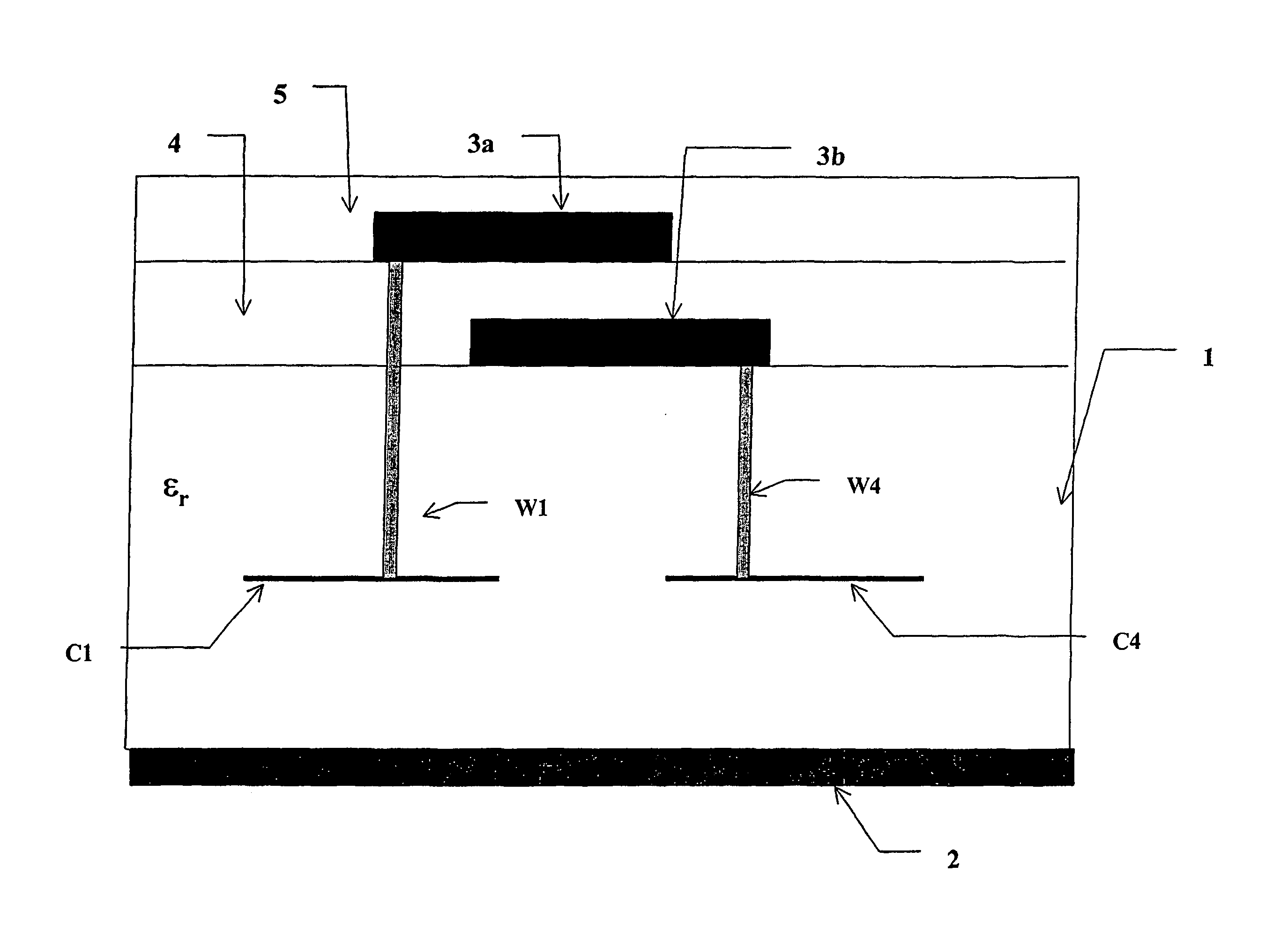
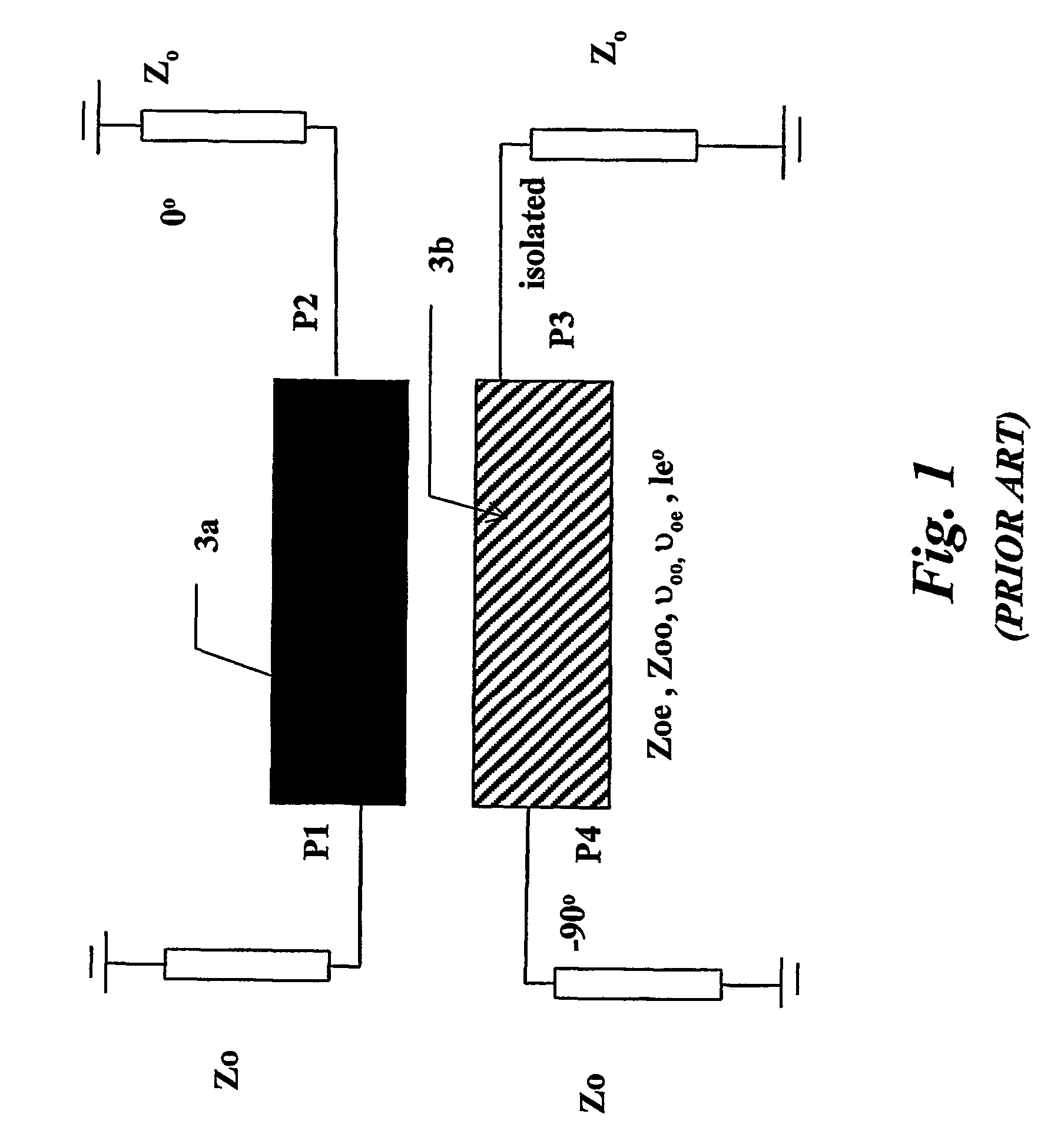
[0054]FIG. 4 shows an equivalent circuit diagram of a coupling device according to the present invention. The arrangement is rather similar to the circuit arrangement as explained as an example with reference to FIG. 1. Thus, the same reference signs denote similar and / or identical components and a repeated explanation thereof is dispensed with.

[0055]The difference between the equivalent circuits shown in FIG. 1 and FIG. 4 resides in that in the circuit according to FIG. 4, grounded capacitors C1 through C4 are connected at the output ports P1 to P4, respectively. With the values of capacitance of the capacitors C1 to C4 being properly chosen, the phase velocity mismatch between odd and even modes can be compensated for, i.e. equalized. The proper values of capacitance of the capacitors C1 to C4 depend on the degree of velocity mismatch. These proper values are determine...


PUM


Abstract

The present invention proposes a coupling device, comprising a substrate (1), a conductive layer (2) covering a first surface of said substrate (1), at least two electromagnetically coupled lines (3a, 3b) being provided opposite to said first surface and at least one thereof being covered by at least one cover layer (4, 5) wherein at least one capacitor (C1, C2, C3, C4) is connected between a first end of at least one of said at least two lines (3a, 3b) and said conductive layer (2). The at least one capacitor is a buried capacitor grounded in order to equalize unequal phase velocities otherwise degrading the performance of e.g. broadside coupled structures in an inhomogeneous substrate structure such as for example microstrips in a multilayer LTCC. Therefore the present invention enables coupling devices having a high performance and offering in that way the best of all possible design scenarios in terms of wideband performance, size and cost.

Description

FIELD OF THE INVENTION[0001]The present invention relates to a coupling device. More particularly, the present invention relates to a coupling device obtainable from a multilayer integrated circuit technology fabrication process.BACKGROUND OF THE INVENTION[0002]Coupling devices (referred to as couplers) in general, such as for example Hybrid 3 dB couplers, are essential circuit components which are increasingly being used for high performance applications in such diverse circuits as RF mixers, amplifiers and modulators. In addition they can be used in a variety of other support functions such as the ones encountered in general RF signal and amplitude conditioning and error signal retrieval systems.[0003]The expression “hybrid” in connection with couplers means an equal split of power between two (output) ports of the coupler with respect to an input port. Hence a 3 dB coupler is a “hybrid” since:10 log(Powerout / Powerin)=−3 dBPowerout / Powerin=10(−3 / 10)=0.5So the output power Powerout...

Claims


Application Information

Patent Timeline
IPC IPC(8): H01P5/18H01L23/538H01L23/64H01L23/66H01P1/00H01P1/203
CPCH01L23/642H01L23/66H01P5/187H01L2924/09701H01L2924/3011H01L2924/0002H01L2924/00
Inventor PASSIOPOULOS, GEORGEAL-TAEI, SARMADZADEH, MAHMOUDLAMACRAFT, KEVINLANE, PHIL
Owner NOKIA CORP
Why Eureka
Try Eureka