[0023]The present invention provides a system and method for incorporating multiple film analysis techniques in a single instrument. This multi-technique capability can enable a user to perform a larger variety of analyses without
purchasing multiple tools. Furthermore, combining the components required for the various analytical techniques in a single tool can lead to design and / or usage efficiencies that can reduce costs and increase
throughput relative to separate single-technique tools.
[0024]According to an embodiment of the present invention, a film analysis system includes both EMP and XRF analysis capabilities. EMP capability is provided by an e-beam generator for directing an e-beam at a sample
coating (i.e., a film or films to be analyzed) and an x-ray detector(s) for measuring characteristic x-rays generated by the sample
coating in response to the source e-beam. The x-ray detector(s) can be either an EDX detector(s), a WDX detector(s), or a combination of both types. XRF capability is provided by a microfocus x-ray tube and an x-ray beam focusing system for focusing a source x-ray beam from the microfocus x-ray tube onto the sample
coating to generate characteristic x-rays via x-ray
fluorescence. These characteristic x-rays can be measured by the same x-ray detector(s) used in the EMP analysis, thereby reducing part count and cost of the film analysis system. Furthermore, the film analysis system beneficially enables rapid EMP analysis for thinner films, while providing the capability for performing XRF analysis for thicker films.
[0025]According to another embodiment of the present invention, a film analysis system includes both GXR and XRF analysis capabilities. GXR capability is provided by a microfocus x-ray tube, a x-ray beam focusing system for focusing the source x-ray beam from the microfocus x-ray tube onto a sample coating (i.e., a film or films to be analyzed), and a position-sensitive detector for measuring the interference pattern generated by the reflected x-rays from the sample coating. The film analysis system also includes a WDX x-ray detector(s) that can perform XRF analysis on the characteristic x-rays emitted by the sample coating in response the portion of the source x-ray beam that is absorbed, rather than reflected, by the sample coating. Because a separate microfocus x-ray tube and x-ray beam focusing system are not required for the XRF analysis, part count and cost of the film analysis system is reduced. Alternatively, a separate microfocus x-ray tube and x-ray beam focusing system for XRF analysis could be included so that operational settings could be optimized for both the GXR and XRF analyses. In either case, combining the two techniques in a single tool advantageously enables accurate GXR thickness measurement coupled with accurate XRF composition measurement. In addition, the film analysis system beneficially enables the GXR and XRF analyses to be performed simultaneously or in rapid succession with each other, thereby improving analysis
throughput. Furthermore, by using a WDX detector(s), the resolution of the XRF analysis is significantly enhanced over conventional tools using an EDX detector(s).
[0026]According to another embodiment of the present invention, a film analysis system includes both GXR and EMP analysis capabilities. GXR capability is provided by a microfocus x-ray tube, a x-ray beam focusing system for focusing the source x-ray beam from the microfocus x-ray tube onto a sample coating (i.e., a film or films to be analyzed), and a position-sensitive detector for measuring the interference pattern generated by the reflected x-rays from the sample coating. EMP capability is provided by an e-beam generator for directing an e-beam at the sample coating, and an x-ray detector(s) for measuring characteristic x-rays generated by the sample coating in response to the source e-beam. The x-ray detector(s) can be either an EDX detector(s), a WDX detector(s), or a combination of both types. By combining the two techniques in a single tool, accurate GXR thickness measurement can be coupled with accurate XRF composition measurement. In addition, the film analysis system beneficially enables the GXR and EMP analyses to be performed simultaneously or in rapid succession, thereby improving analysis throughput.
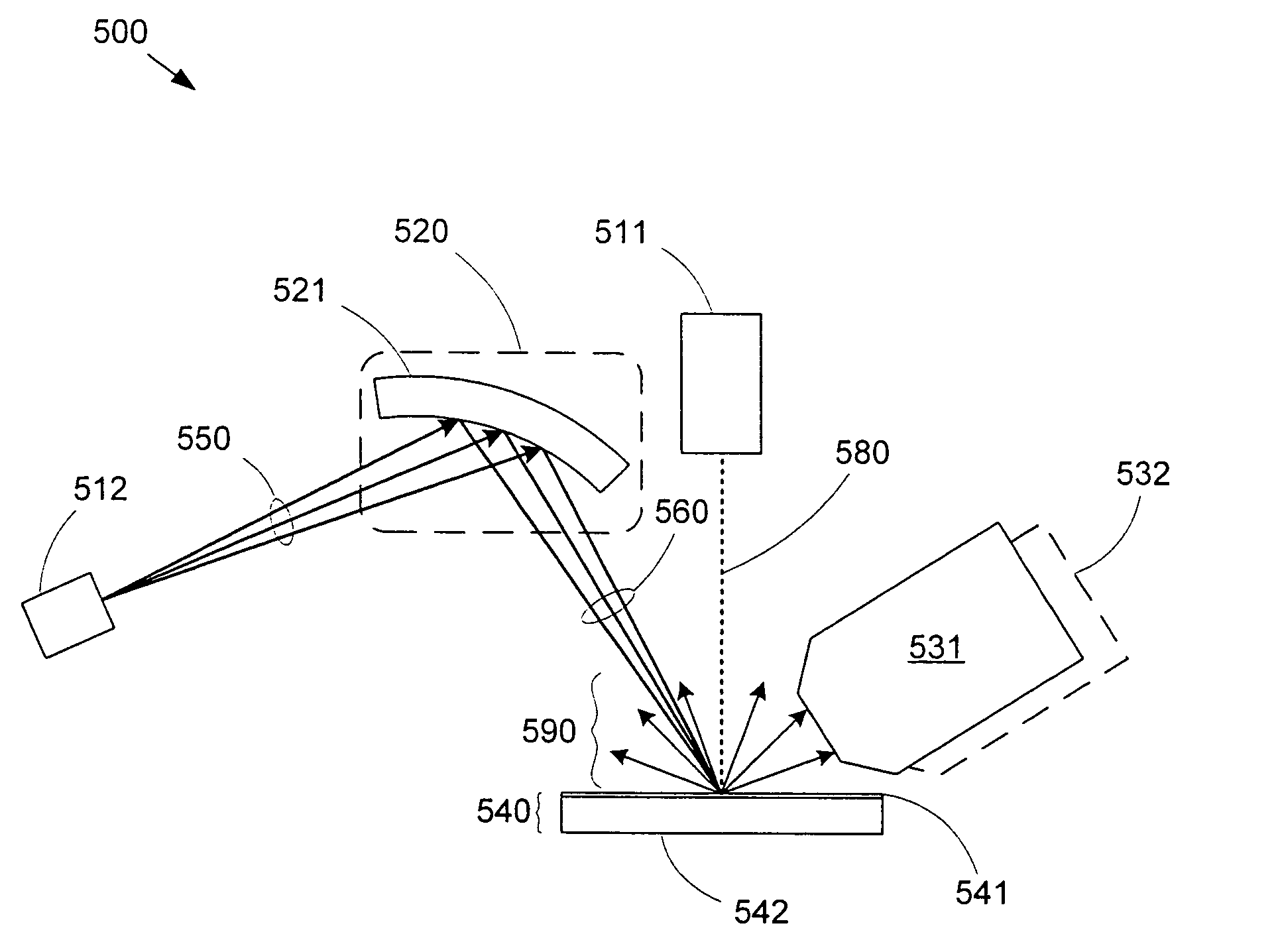
[0027]According to another embodiment of the present invention, a film analysis system includes GXR, XRF, and EMP analysis capabilities. GXR capability is provided by a microfocus x-ray tube, a x-ray beam focusing system for focusing the source x-ray beam from the microfocus x-ray tube onto a sample coating (i.e., a film or films to be analyzed), and a position-sensitive detector for measuring the interference pattern generated by the reflected x-rays from the sample coating. EMP capability is provided by an e-beam generator for directing an e-beam at the sample coating, and an x-ray detector(s) for measuring characteristic x-rays generated by the sample coating in response to the source e-beam. The x-ray detector(s) can be either an EDX or WDX detector(s). To minimize component count, XRF capability can be provided by properly selecting and configuring the microfocus x-ray tube, so that a portion of the source x-ray beam is absorbed by the sample coating. The characteristic x-rays emitted by the sample coating in response to the absorbed source x-rays can then be measured by the x-ray detector(s) (used also in for EMP analysis). Alternatively, to optimize XRF and GXR performance, a second microfocus x-ray tube can be included to generate the source x-ray beam for XRF analyses. In any case, combining all three techniques in a single tool provides maximum flexibility in film analysis, and allows for component count reduction and / or throughput enhancement, as described with respect to the aforementioned embodiments.

