Methods of forming power semiconductor devices having laterally extending base shielding regions

a shielding region and semiconductor technology, applied in semiconductor devices, diodes, electrical apparatus, etc., can solve the problems of a relatively low high-frequency figure-of-merit (hfom) and a lower than-ideal uniform concentration of doping in the drift region,

Inactive Publication Date: 2006-05-09
SEMICON COMPONENTS IND LLC
View PDF102 Cites 24 Cited by
  • Summary
  • Abstract
  • Description
  • Claims
  • Application Information

AI Technical Summary

Benefits of technology

[0016]According to further aspects of the first embodiment, enhanced forward on-state and reverse blocking characteristics can be achieved by including highly doped shielding regions of second conductivity type that extend in the mesa and on opposite sides of the transition region. In particular, a first shielding region of second conductivity type is provided that extends between the first base region and the drift region and is more highly doped than the first base region. Similarly, a second shielding region of second conductivity type is provided that extends between the second base region and the drift region and is more highly doped than the second base region. To provide depletion during forward on-state and reverse blocking modes of operation, the first and second shielding regions form respective P-N rectifying junctions with the transition region. High breakdown voltage capability may also be achieved by establishing a product of the peak first conductivity type dopant concentration in the transition region and a width between the first and second shielding regions in a range between 1×1012 cm−2 and 7×1012 cm−2.
[0021]The step of implanting shielding region dopants is also preferably preceded by the step of forming trenches in the semiconductor substrate and lining the trenches with trench insulating layers. Conductive regions are also formed on the trench insulating layers. These trench related steps may be performed before the step of implanting the transition region dopants. In this case, the transition region dopants are preferably implanted into the conductive regions within the trenches and into mesas that are defined by the trenches. According to still further preferred aspects of this embodiment, steps are also performed to increase maximum on-state current density within the power device by improving the configuration of the source contact. In particular, the source contact is formed on a sidewall of the trenches by etching back the trench insulating layers to expose the source, base and shielding regions and then forming a source contact that ohmically contacts the conductive regions and also contacts the source, base and shielding regions at the sidewall of each trench.
[0023]A second base region and a second base shielding region may also be provided in the substrate. In particular, the first and second base regions may be self-aligned to first and second opposing ends of the insulated gate electrode and may form respective P-N junctions with opposing sides of an upper portion of the transition region extending adjacent the first surface. The first and second base shielding regions are more highly doped than the first and second base regions and extend laterally towards each other in the semiconductor substrate to thereby constrict a neck of the upper portion of said transition region to a minimum width at a second depth relative to the first surface. The second depth is preferably greater than about 0.25 microns. A product of the peak first conductivity type dopant concentration in the transition region and a width of the transition region at the first depth is preferably in a range between about 1×1012 cm−2 and about 7×1012 cm−2, and more preferably in a range between about 3.5×1012 cm−2 and about 6.5×1012 cm−2.

Problems solved by technology

However, the performance of these devices was limited by the fact that the forward blocking voltage must be supported across the gate oxide at the bottom of the trench.
However, in this device a lower-than-ideal uniform doping concentration in the drift region was required to compensate for the high concentration of field lines near the bottom corner of the trench when blocking high forward voltages.
Notwithstanding these excellent characteristics, the transistor of FIG. 3 of the '898 patent may suffer from a relatively low high-frequency figure-of-merit (HFOM) if the overall gate-to-drain capacitance (CGD) is too large.
Improper edge termination of the MOSFET may also prevent the maximum blocking voltage from being achieved.
However, as described below, power MOSFETs including LDMOS transistors, may have non-linear characteristics that can lead to signal distortion.
This non-linearity can lead to signal distortion in power amplifiers.

Method used


Image

  • Methods of forming power semiconductor devices having laterally extending base shielding regions
  • Methods of forming power semiconductor devices having laterally extending base shielding regions
  • Methods of forming power semiconductor devices having laterally extending base shielding regions

Examples


Embodiment Construction

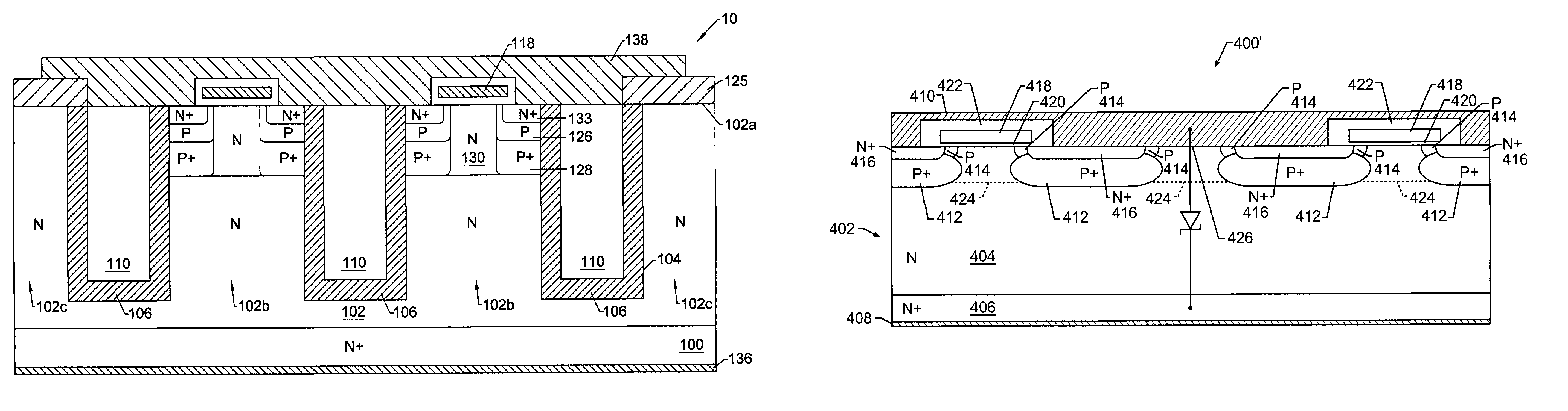
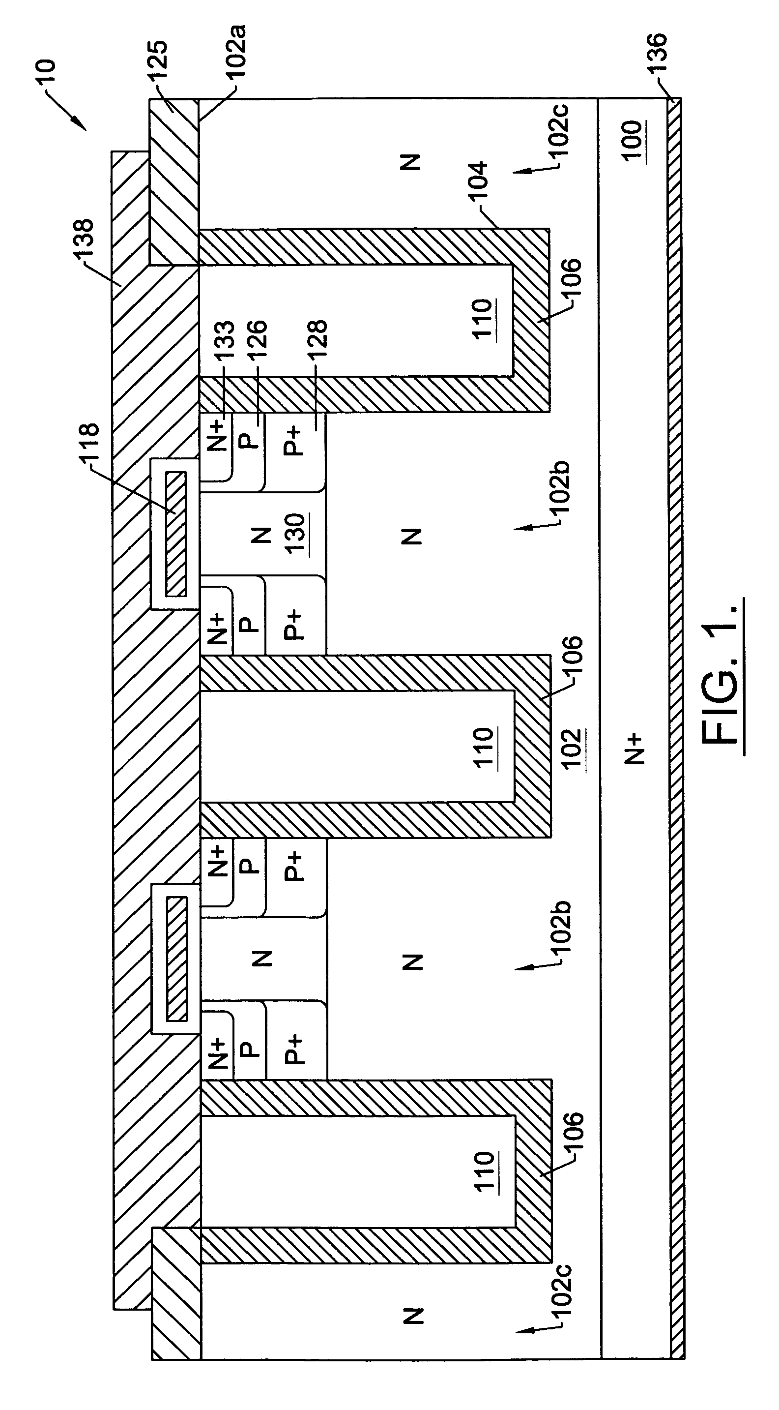
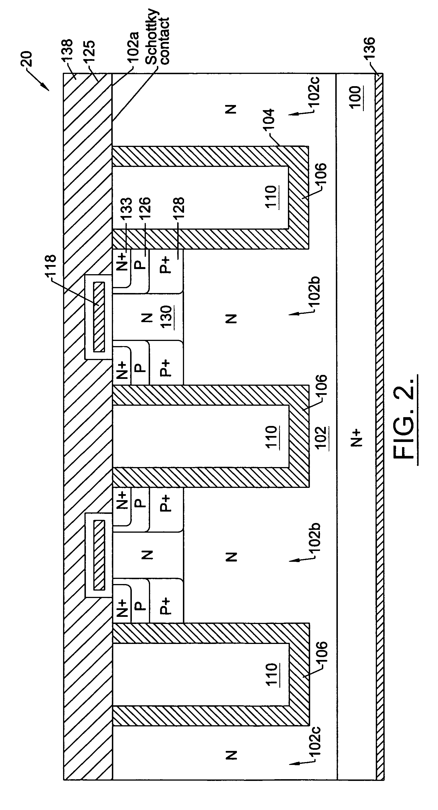
[0042]The present invention will now be described more fully hereinafter with reference to the accompanying drawings, in which preferred embodiments of the invention are shown. This invention may, however, be embodied in different forms and should not be construed as limited to the embodiments set forth herein. Rather, these embodiments are provided so that this disclosure will be thorough and complete, and will fully convey the scope of the invention to those skilled in the art. In the drawings, the thickness of layers and regions are exaggerated for clarity. It will also be understood that when a layer is referred to as being “on” another layer or substrate, it can be directly on the other layer or substrate, or intervening layers may also be present. Moreover, the terms “first conductivity type” and “second conductivity type” refer to opposite conductivity types such as N or P-type, however, each embodiment described and illustrated herein includes its complementary embodiment as...


PUM


Abstract

Methods of forming power semiconductor devices include forming a semiconductor substrate having a drift region of first conductivity type therein and a transition region of first conductivity type that extends between the drift region and a first surface of the semiconductor substrate. A gate electrode is formed on the first surface. Base and base shielding region dopants are implanted into the transition region using the gate electrode as an implant mask. A plurality of annealing steps are performed so that the base shielding region dopants are driven in laterally and vertically to substantially their full and final depth within the substrate and thereby define first and second base shielding regions that constrict a neck of the transition region to a minimum width.

Description

REFERENCE TO PRIORITY APPLICATIONS[0001]This application is a continuation of U.S. application Ser. No. 10 / 671,333, filed Sep. 24, 2003 now U.S. Pat. No. 6,800,897, which is a continuation-in-part of U.S. application Ser. No. 10 / 008,171, filed Oct. 19, 2001 now U.S. Pat. No. 6,791,143, which is a continuation-in-part of application Ser. No. 09 / 833,132, filed Apr. 11, 2001 now U.S. Pat. No. 6,781,194, the disclosures of which are hereby incorporated herein by reference.FIELD OF THE INVENTION[0002]The present invention relates to semiconductor switching devices, and more particularly to switching devices for power switching and power amplification applications and methods of forming same.BACKGROUND OF THE INVENTION[0003]Power MOSFETs have typically been developed for applications requiring power switching and power amplification. For power switching applications, the commercially available devices are typically DMOSFETs and UMOSFETs. In these devices, one main objective is obtaining a...

Claims


Application Information

Patent Timeline
Patent Type & Authority Patents(United States)
IPC IPC(8): H01L21/336H01L21/332H01L21/4763H01L21/76H01L29/06H01L29/08H01L29/10H01L29/40H01L29/417H01L29/78H01L29/872
CPCH01L29/0878H01L29/1095H01L29/407H01L29/872H01L29/66727H01L29/7802H01L29/7806H01L29/0847H01L29/402H01L29/41766H01L29/41741
Inventor BALIGA, BANTVAL JAYANT
Owner SEMICON COMPONENTS IND LLC
Why Eureka
Try Eureka