
Low-voltage, low-power transimpedance amplifier architecture

a transimpedance amplifier and low-power technology, applied in the field of analog circuit architecture, can solve the problems of difficult to sustain a constant collector current, large input impedance of the voltage gain stage, and difficult to achieve constant collector current, and achieve the effect of reducing the number of stacked devices, reducing power consumption, and reducing supply voltag

Inactive Publication Date: 2006-05-09
CORNELL RES FOUNDATION INC
View PDF9 Cites 21 Cited by
  • Summary
  • Abstract
  • Description
  • Claims
  • Application Information

AI Technical Summary

Benefits of technology

"The present invention is about circuits that convert input current to output voltage using a special design. The circuit includes a current buffer and a direct drive of the buffer output into an impedance to convert the current signal to a voltage signal. The circuit has low power consumption and operates at high speeds. The use of transistors as current buffers allows for wider band operation than traditional circuits. The invention is not limited to NMOS transistors and can also use other types of transistors or bipolar junction transistors. The technical effects of the invention are improved performance stability and reduced power consumption."

Problems solved by technology

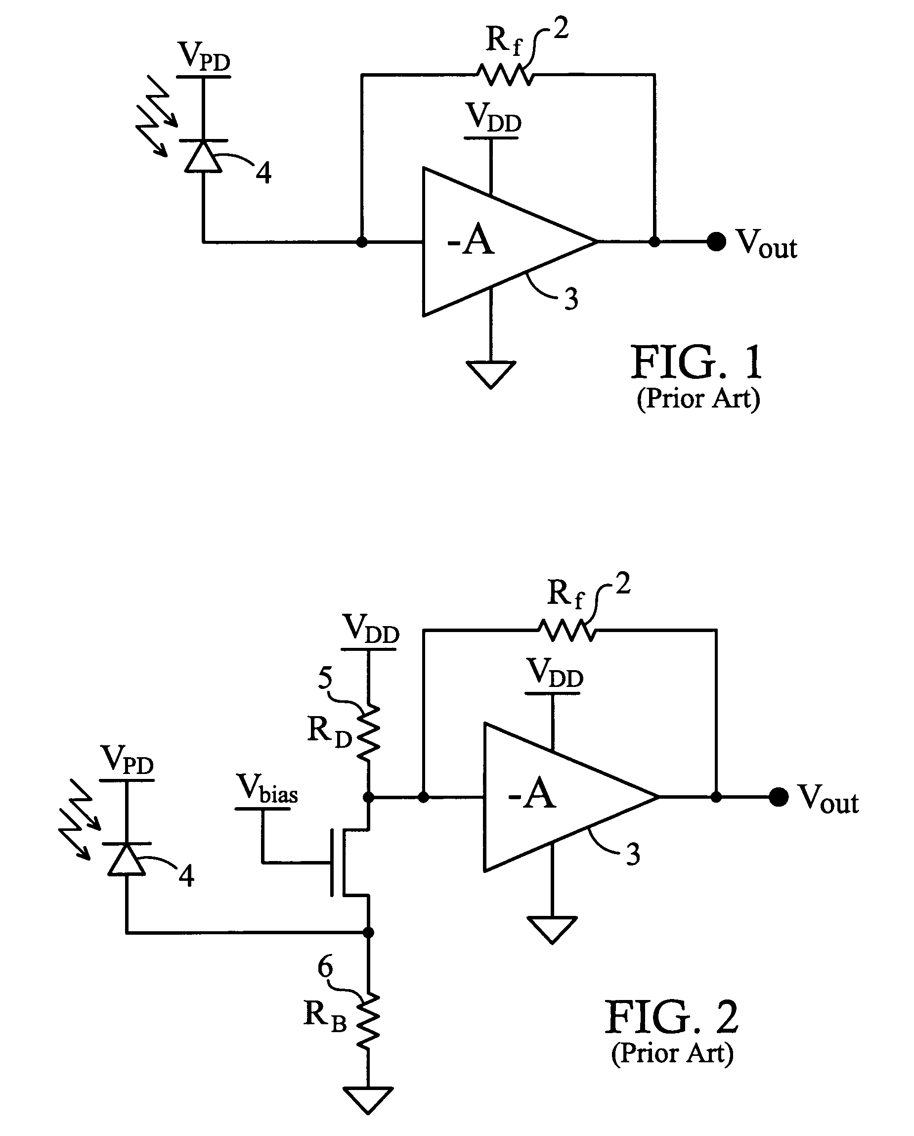
This approach has some deficiencies for low-power, low-voltage systems at high data rates.
The main problem with this approach is that, for correct operation, the input impedance of the voltage gain stage must be large.
Further, the performance of such systems is limited by the performance of the voltage gain stage, which strongly effects the power consumption, the bandwidth and the required power supply voltage for the overall TIA.
This problem is amplified by the exponential response of the current to Vbe variations in a bipolar technology, which may make it difficult to sustain a constant collector current in a common base (CB) stage configuration with variations in DC photodiode current for a DC coupled system.
That fairly complex architecture has a relatively high power consumption and larger chip area and may require the use of a higher voltage supply to accommodate the error amplifier.
DC coupling is desirable for short-haul systems, as AC coupling may require data coding and coding results in undesired overhead (latency, power and chip area).
DC coupling can present problems in receivers due to variations in the DC input current with input signal power level affecting the bias conditions of the TIA.

Method used


Image

  • Low-voltage, low-power transimpedance amplifier architecture
  • Low-voltage, low-power transimpedance amplifier architecture
  • Low-voltage, low-power transimpedance amplifier architecture

Examples


Embodiment Construction

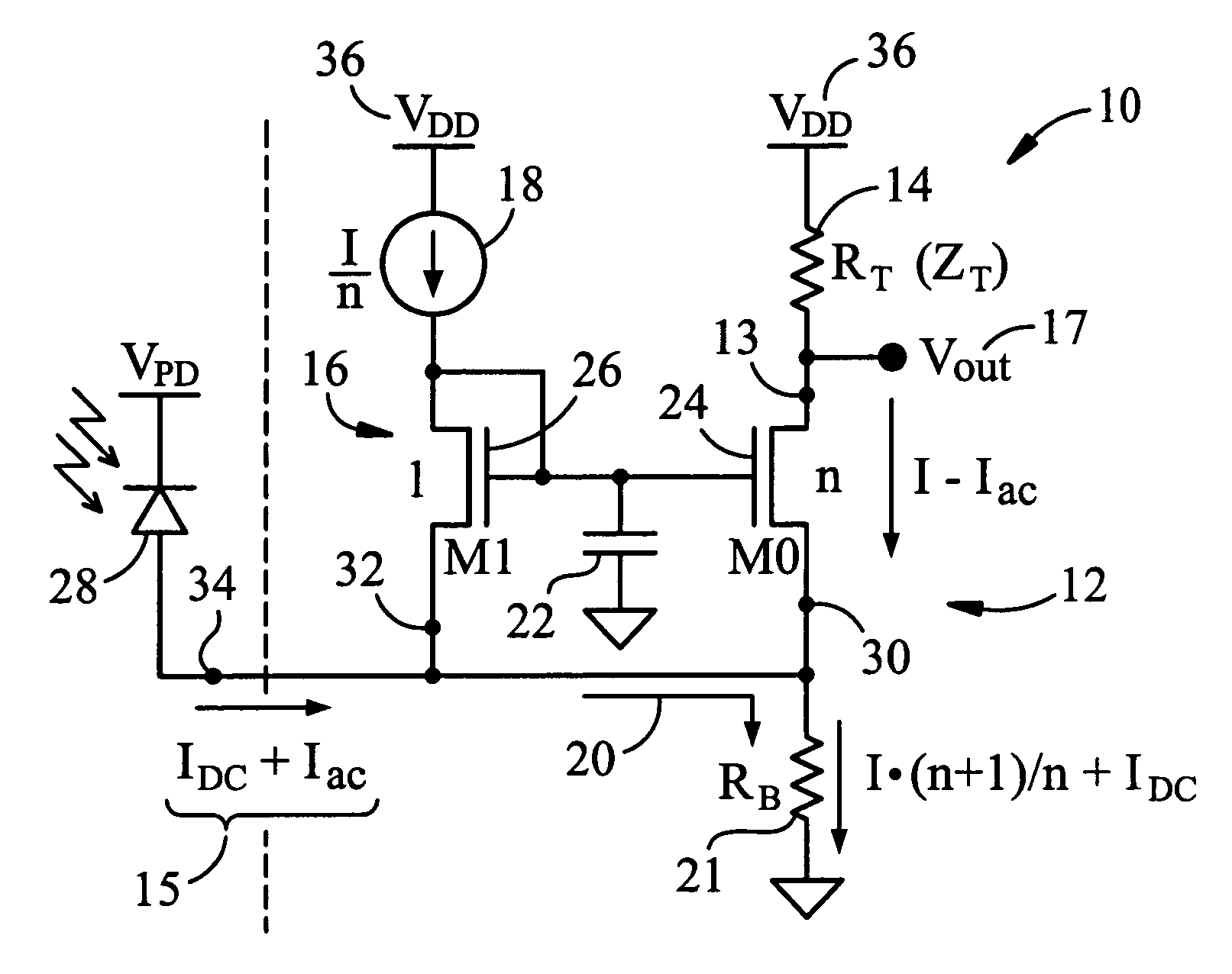
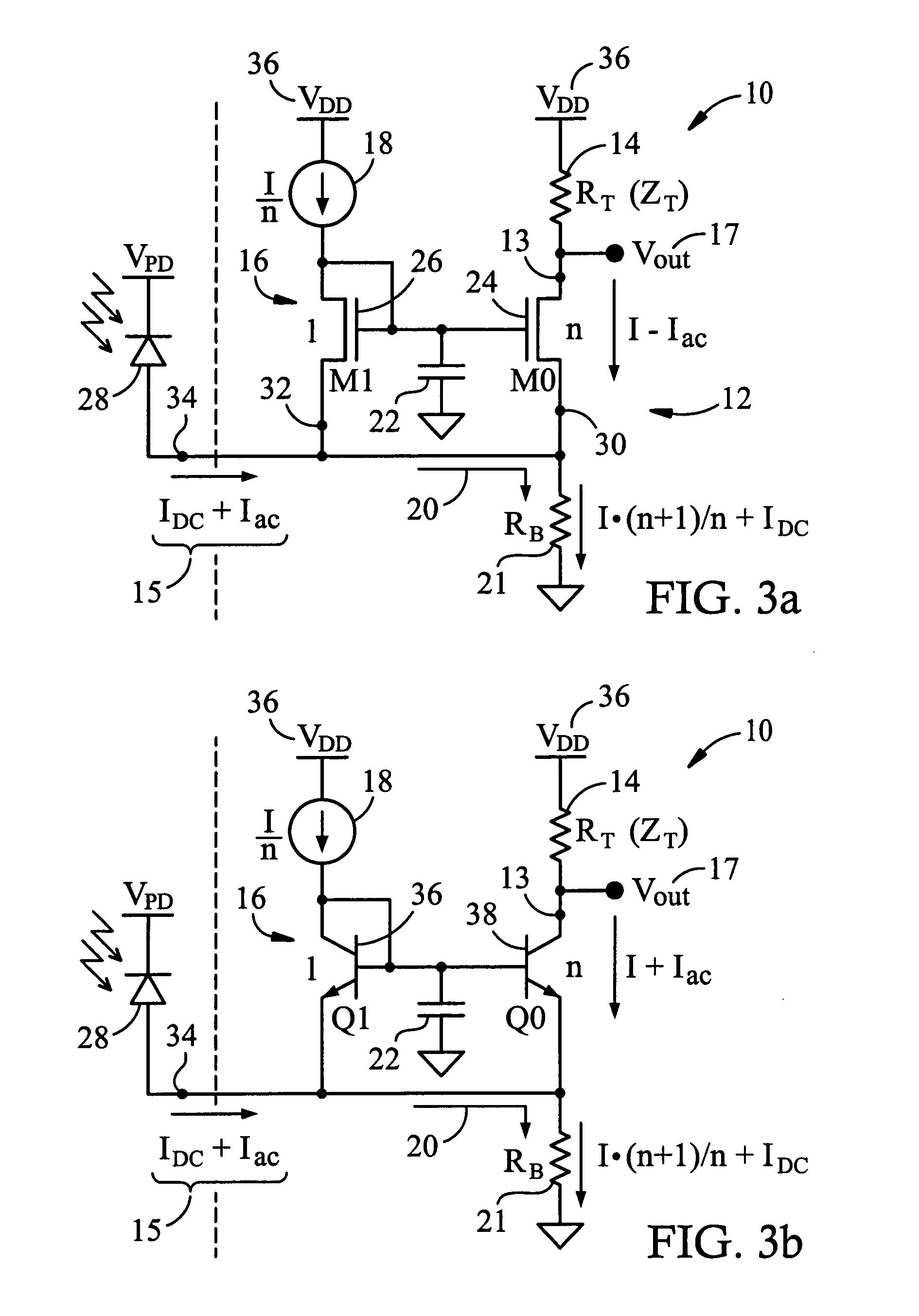
[0022]In a first aspect, the present invention provides transimpedance amplifier (TIA) architectures for converting an input current to a voltage. In the description below, references are made to CMOS and bipolar implementations of the TIA architectures as reflected, respectively, in FIGS. 3a and 3b. Any disparity in the amount of text devoted to one implementation or the other arises solely from the desire for clarity, and is in no manner meant to be limiting. The concepts described apply equally well to both of these families of implementation as well as to implementations that employ devices sharing the characteristics of such transistors. The term “transistor” as used herein encompasses any device that provides a controllable output current when a voltage difference is present across its terminals, the output being current-, voltage-, optically- or mechanically-controlled. Any significant differences in alternative implementations are noted. Among alternative MOSFET embodiments,...


PUM


Abstract

Circuits for converting an input current to an output voltage that employs a uniquely biased common-gate or common-base stage as a current buffer and a direct drive of the current buffer output into an impedance to convert the current signal to a voltage signal.

Description

BACKGROUND OF THE INVENTION[0001]This invention relates generally to analog circuit architecture, and, more particularly to broadband transimpedance amplifiers for converting currents to voltages.[0002]Current trends toward the integration of electro-optic interfaces with high-speed digital integrated circuits for local and / or storage area networks and other short-haul applications require low-voltage interface circuits that can operate from available digital supplies. In order to make arrays of these interconnects efficient and a feasible alternative to electrical interconnects in server and mainframe applications, low power consumption must be also achieved. (See A. Schild, et al., “Amplifier Array for 12 Parallel 10 Gb / s Optical-Fiber Links Fabricated in a SiGe Production Technology”, 2002 IEEE RFIC Symposium, pp. 89–92, 2002, incorporated herein by reference.) To avoid coding requirements for the transmitted data, a DC-coupled interface is desirable. To meet these requirements, ...

Claims


Application Information

Patent Timeline
Patent Type & Authority Patents(United States)
IPC IPC(8): H03F3/08H03F3/343H03F3/347
CPCH03F3/08H03F3/347H03F3/343H03F2200/513
Inventor GUCKENBERGER, DREWKORNEGAY, KEVIN T.
Owner CORNELL RES FOUNDATION INC
Learn More