Method to reduce inductive effects of current variations by internal clock phase shifting

a technology of internal clock phase and current variation, which is applied in the direction of voltage/current interference elimination, pulse technique, and increase in modification, can solve the problems of large current spikes on the power net of the ic, inductive voltage transients, and current flow consumes electric power, so as to reduce current transitions and minimize inductive voltage transients , the effect of more reliable operation of the i

Active Publication Date: 2006-05-16
TELOGY NETWORKS
View PDF2 Cites 3 Cited by
  • Summary
  • Abstract
  • Description
  • Claims
  • Application Information

AI Technical Summary

Benefits of technology

[0011]Modules are decoupled from each other's clock domains during information processing and subsequently re-coupled for further operational activity these isolated modules are managed on a timing scheme separate from each other without detrimental effects to the transmission of binary information. Separate clocks are generated for and coupled with these now isolated modules, such that the timing of the signal switching is managed to be out of step throughout the chip, lowering the cumulative effects of multi-module simultaneous switching and reducing unwanted interference from the associated voltage transients.
[0012]By combining decoupling / re-coupling with clock signal delay management the present invention teaches a solution for reducing chip operating voltage and power consumption without reducing signal integrity.
[0013]Therefore, to reduce the voltage transient influences associated with low level voltage signal transmission in high density ICs, and as a way to enhance the state of the art, the present invention is a method of reducing switching noise by eliminating as many simultaneous switches as possible. This is accomplished through a chip design based on decoupling of IC module clock domains and introducing same-frequency but phase-shifted clock signals to each independent domain.
[0014]To eliminate large voltage transients caused by a plurality of binary signals switching simultaneously, the present invention discloses a method of IC chip design which eliminates simultaneous signal switching wherever possible. This is accomplished by decoupling relatively independent functional units within the IC from the IC clock and generating out-of-phase clocks to each independent unit.
[0016]This will result in the timing of the signal switching of each decoupled module being non-concurrent with the signal switching from all of the other decoupled modules. Changes in switch-generated current demand will likewise be offset. At the chip level, these offset current changes will be spread out in time and will be much smaller in magnitude. The reduced current transitions will minimize the inductive voltage transients, helping to maintain signal integrity and resulting in a more reliable operation of the IC.
[0017]The proposed decoupling-by-design and clock signal management approach herein described thus provides the opportunity to create high density ICs comprising independently segregated or modularized circuits, each of which utilize slightly out-of-phase switching in their bit processing operations. This offset switching can greatly reduce large, simultaneous current changes and their resultant deleterious voltage transients. The details of the integrated circuit layout would be subject to the designer and purpose of the chip, but the nature of the concept is described hereunder.

Problems solved by technology

This current flow consumes electric power.
This creates situations in which a large amount of current is being used at relatively low voltage (currently about 1.0V) in very tightly configured integrated circuitry.
Since all synchronous IC circuits are typically coordinated by the same internal clock, all of the transistors that draw power during switching do it at the same time, resulting in large current spikes on the power net of the IC.
As anyone skilled in the art of integrated circuit design is aware, sudden changes in current within a circuit results in inductive voltage transients.
Large current spikes can produce voltage transients which are outside the operating range tolerance and can lead to false signals and operational failures.
While helpful, these design techniques cannot eliminate the voltage transients caused by large current changes and have no effect on the voltage transients caused by the inductance on the IC power net from the package pins to the silicon.
Multi-chip module packaging further exacerbates this problem.
As multi-tasking operations progress under the influence of the synchronizing chip clock, the incidence of simultaneous signal (current) changes and their attendant voltage transients increases.

Method used


Image

  • Method to reduce inductive effects of current variations by internal clock phase shifting
  • Method to reduce inductive effects of current variations by internal clock phase shifting
  • Method to reduce inductive effects of current variations by internal clock phase shifting

Examples


Embodiment Construction

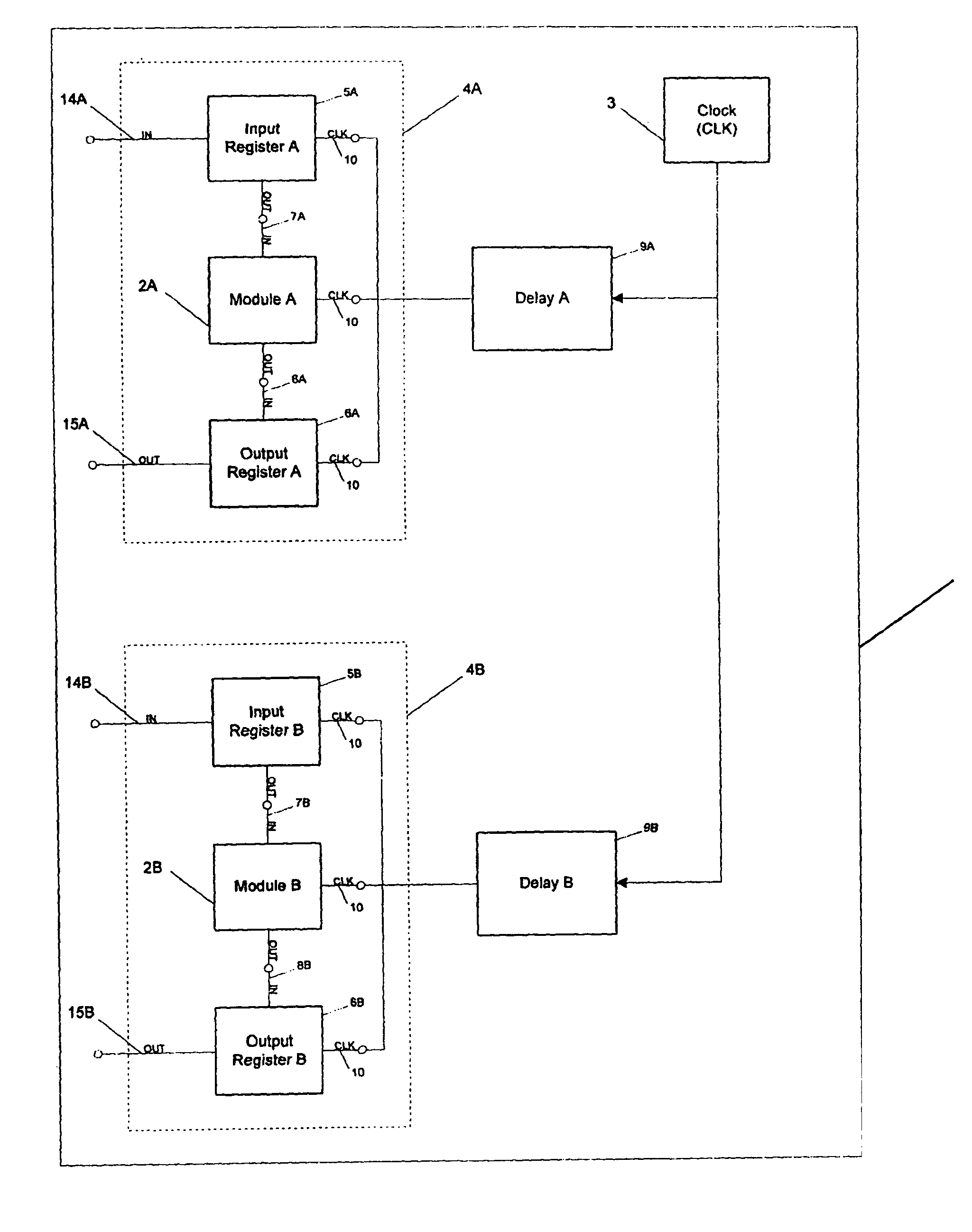
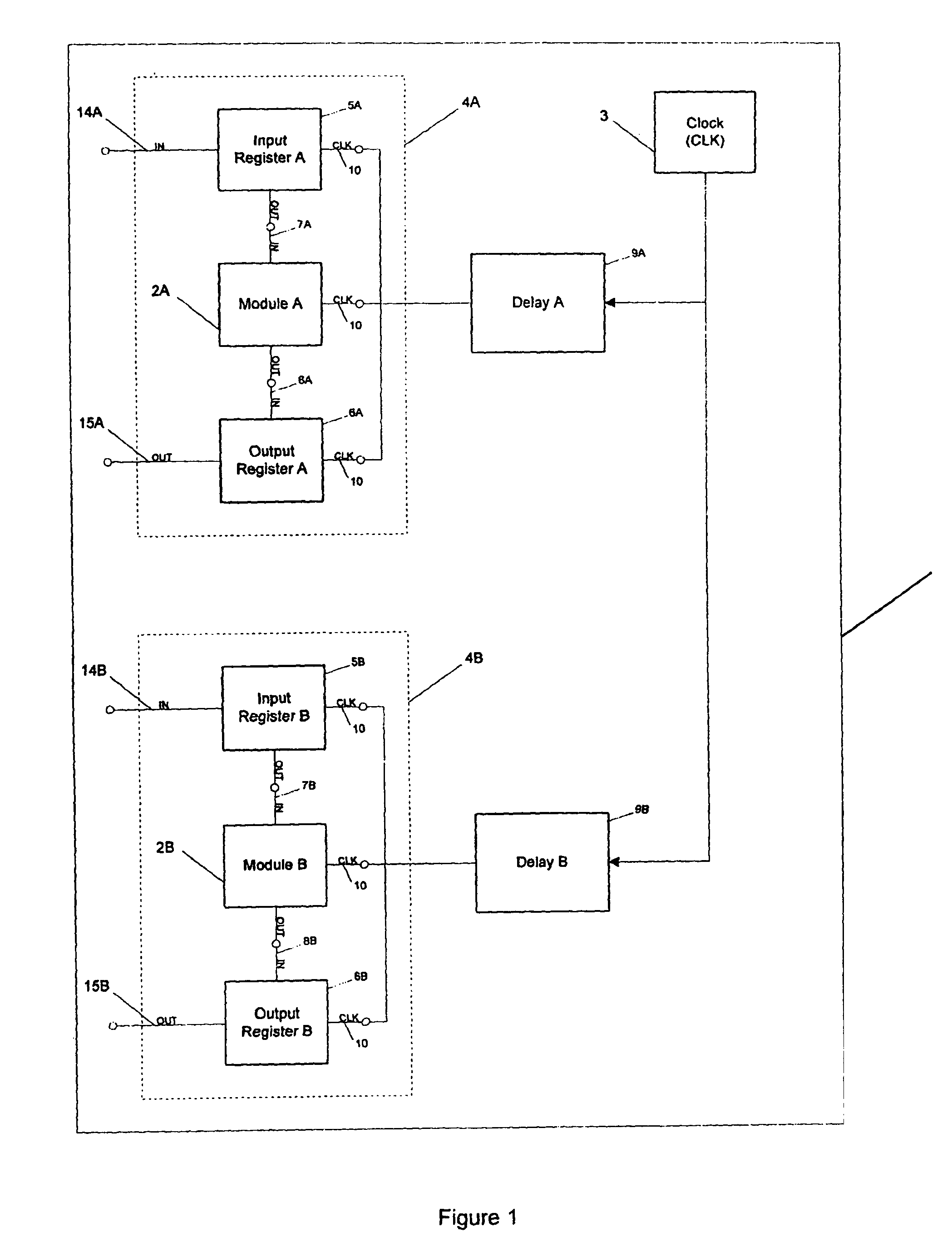
[0021]In the preferred embodiment of the present invention, the design of an electronic integrated circuit (IC) such as a CPU microprocessor comprises reasonably independent synchronous functional modules as well as a synchronizing clock generator. The modules may include arithmetic logic units, control units or any other suitably separable units. FIG. 1 conceptually illustrates an IC chip 1 with modules A and B (2A and 2B) and on-chip clock 3. During chip design, operational boundaries 4A and 4B are identified around said modules such that binary signals may be processed internal thereto subject to a minimum of interface with the remainder of the IC.

[0022]The exemplary embodiment discloses an IC device having two independent functional modules. The method of the invention can be employed on devices comprising any number of relatively independent and separable circuits without departing from the scope of the present invention. The selection of the proper operational boundaries betwe...


PUM


Abstract

Modularized clock decoupling and signal delay management is provided for the purpose of reducing simultaneous binary signal switch-induced inductive voltage transients in lower voltage synchronous semiconductor devices. The voltage levels in low-voltage devices must be tightly maintained for proper transistor logic operations. Signal switching results in current changes on the power net of an IC. Current changes produce inductive voltage transients which propagate throughout the device and which can interfere with signal transmission and device operation. Relatively independent functioning circuits of an integrated circuit are isolated from the chip clock and each isolated circuit module is provided with its own independent, same-frequency, but slightly out-of-phase clock signal. Signal switching within any module is thus occurring out-of-phase with that of all other modules and, as a result, switch-associated voltage transients are limited to those associated with one module's circuits at a time.

Description

FIELD OF THE INVENTION[0001]The present invention relates to the field of design and operation of binary signal switching in integrated circuits. More specifically, the present invention is a method to reduce inductive effects caused by a plurality of electronic gates switching simultaneously within an IC.BACKGROUND OF THE INVENTION[0002]Semiconductor integrated circuit (IC) devices utilize a pair of voltage levels—one higher and one lower, in the performance of their data processing operations. Toggling between the voltage levels serves as a binary signal—“1” at the higher voltage level or “0” at the lower voltage level. The signal is “read” by transistors and propagated throughout the device. In response to these voltage changes, current flows across the power net of the device flowing to and through its multitude of transistors according to the logical design of the circuit. This current flow consumes electric power.[0003]As demand for greater capacity and performance in an ever ...

Claims


Application Information

Patent Timeline
Patent Type & Authority Patents(United States)
IPC IPC(8): H03K17/16
CPCH03K19/00346
Inventor KRASNANSKY, KEITH GERARDDRAFZ, RONALD
Owner TELOGY NETWORKS
Why Eureka
Try Eureka