Semiconductor integrated circuit device with test data output nodes for parallel test results output

a technology of integrated circuit devices and test data, which is applied in the direction of solid-state devices, semiconductor/solid-state device details, instruments, etc., can solve the problems of increasing test costs, reducing the number of devices which can be measured simultaneously, and unable to perform write operations on this comparison data inpu

Inactive Publication Date: 2006-05-16
RENESAS ELECTRONICS CORP
View PDF8 Cites 12 Cited by
  • Summary
  • Abstract
  • Description
  • Claims
  • Application Information

AI Technical Summary

Benefits of technology

[0131]It is an object of the present invention to provide a semiconductor integrated circuit device capable of continuously testing a normal column space and a spare column space of a DRAM core.

Problems solved by technology

Further, even if test may be possible, the number of devices which can be measured simultaneously decreases to increase test cost because of the large number of signal / data lines from one device under test.
It is noted, however, if it is required to input comparison data at an earlier cycle than that of the application of the read command because of the restriction of the number of stages of delays for generating comparison data internally, a restriction that the write operation cannot be performed on this comparison data inputted, or other occurs.
If the spare data bit is read together with the other fixed data and applied to the external tester, such a problem arises that the test cannot be performed while successively accessing a spare column address space and a normal column address space, as will be described in the following.
Therefore, if such fail bits are stored in the spare column address space, the entire of the spare column address region is always determined to be fail and the repair determination cannot be accurately made.
If pass / fail bit information is disposed in a distributed manner in this fail / bit memory in accordance with the test terminals, in particular, fail bits F are distributed in accordance with the respective terminals and mixed with data for the normal memory cells, making it even more difficult to specify a fail memory cell.
Thus, high speed operation cannot be ensured and data indicating the pass / fail state of the spare memory cell cannot be stored at real time.
Moreover, to arrange the selector used only in a memory test for repair determination in the tester, it is necessary to modify the tester, resulting in troublesome labor for such arrangement.
With the configuration in which memory cell rows are shared by normal memory cells and spare memory cells, it takes disadvantageously long time to perform the test.
Therefore, if the normal column address space and the spare column address space are separately tested, test time is disadvantageously lengthened because of this pause time and product cost is disadvantageously increased.

Method used


Image

  • Semiconductor integrated circuit device with test data output nodes for parallel test results output
  • Semiconductor integrated circuit device with test data output nodes for parallel test results output
  • Semiconductor integrated circuit device with test data output nodes for parallel test results output

Examples


first embodiment

[First Embodiment]

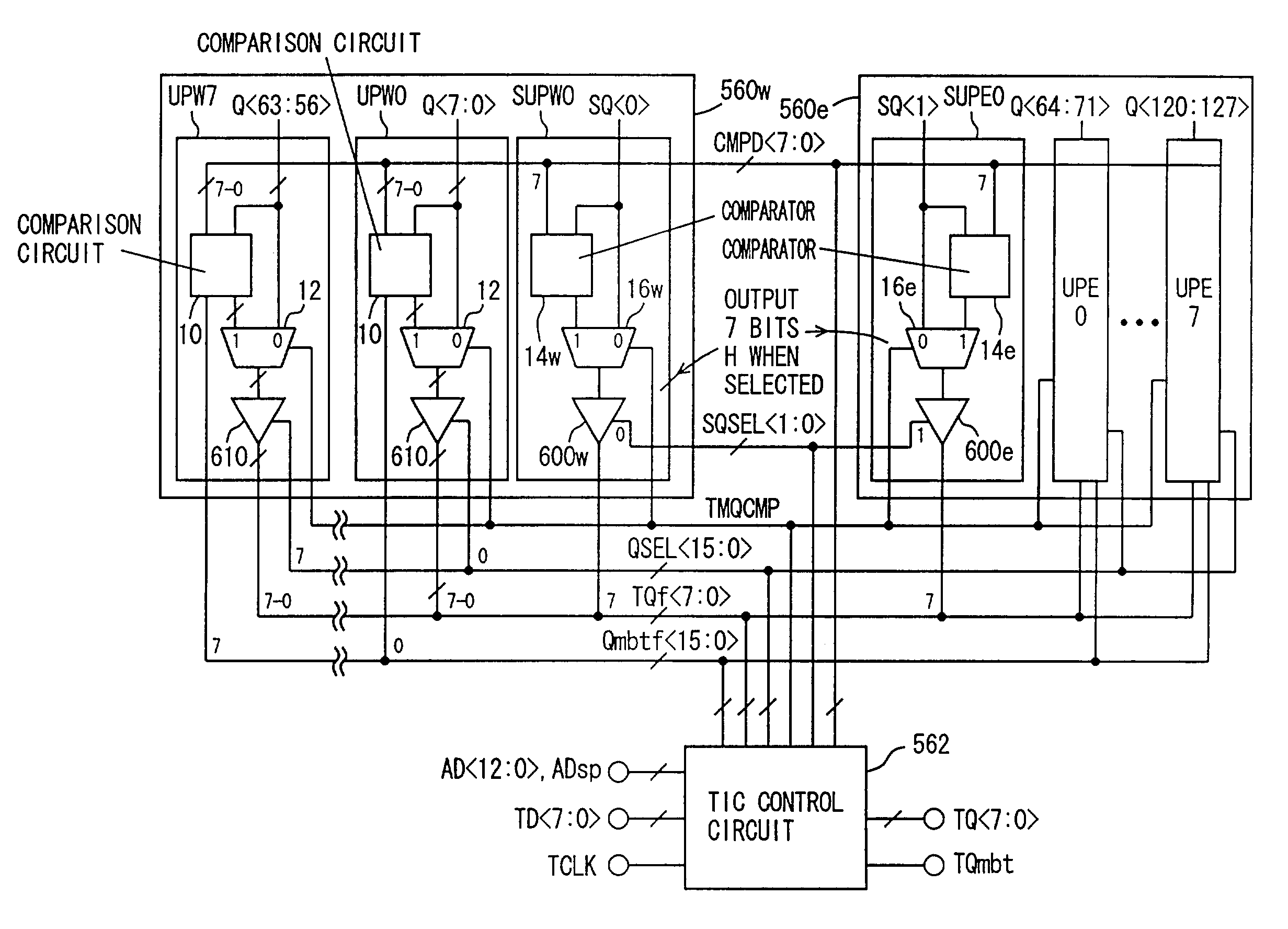
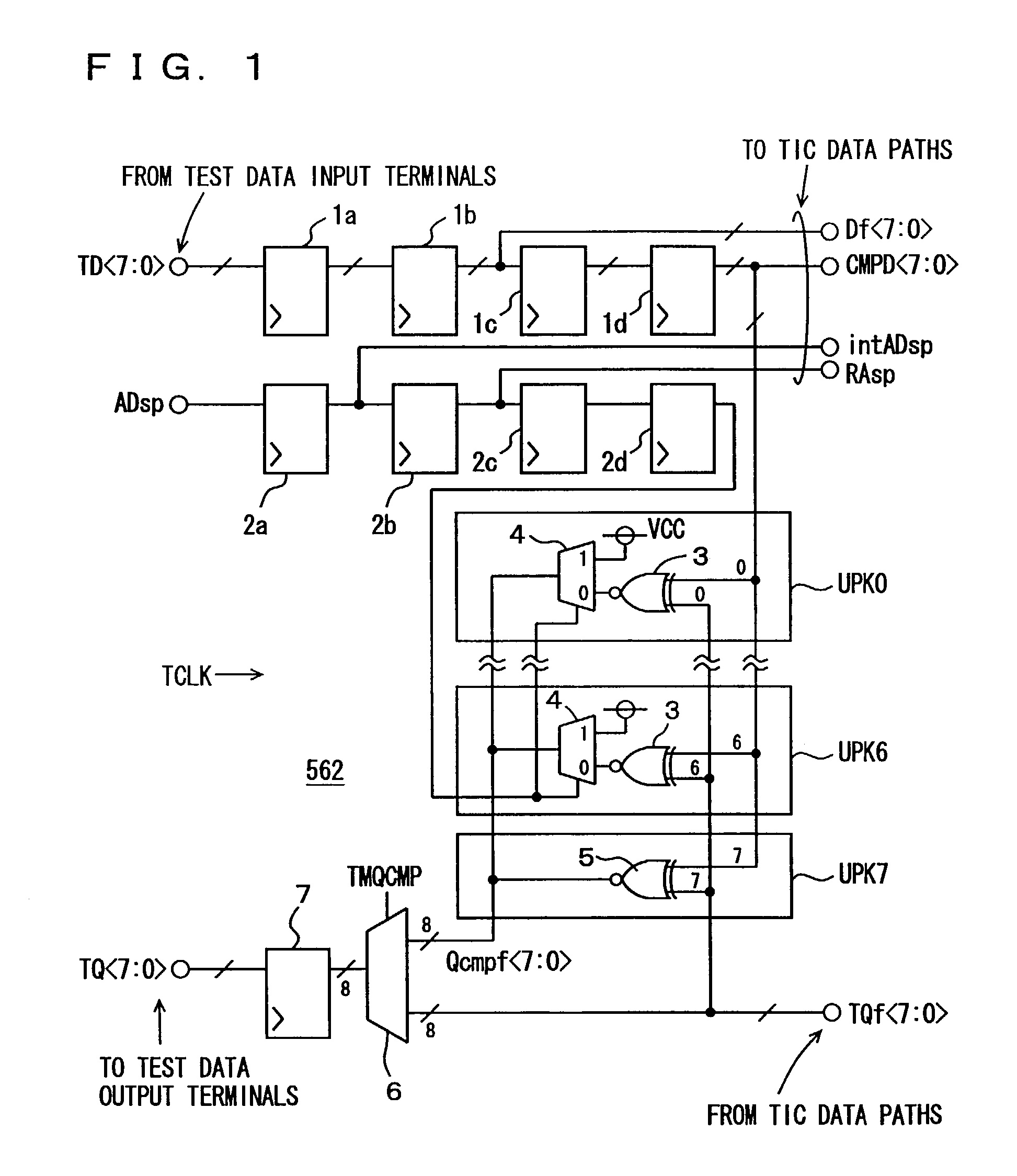
[0162]FIG. 1 is a schematic diagram showing the configuration of the main portion of TIC control circuit 562 according to the first embodiment of the present invention. In FIG. 1, TIC control circuit 562 includes: four stages of flip-flops 1a to 1d which transfer test data TD of 8 bits applied from a test data input terminals (nodes) synchronously with test clock signal TCLK; cascaded flip-flops 2a to 2d of four stages which transfer spare space addressing address signal ADsp synchronously with test clock signal TCLK; unit processing circuits UPK0 to UPK7 which receive the respective bits of test read data TQf of 8 bits from a TIC data path, not shown; a select circuit 6 which selects one of data Qcmpf of 8 bits and test read data TQf of 8 bits from unit processing circuits UPK0 to UPK7 in accordance with a test mode instructing signal TMQCMP; and a flip-flop 7 which transfers output signal of 8 bits from select circuit 6 synchronously with test clock signal TCLK a...

second embodiment

[Second Embodiment]

[0196]FIG. 3 is a schematic diagram showing the configuration of a main portion of TIC control circuit 562 according to the second embodiment of the present invention. In TIC control circuit 562 shown in FIG. 3, output signal Qcmpf of 8 bits of unit processing circuits UPK0 to UPK7 is applied to flip-flop 7. Select circuit 6 shown in FIG. 4 is not used. Since the remaining configuration shown in FIG. 3 is the same as that shown in FIG. 1, corresponding parts are denoted by the same reference symbols and will not be described in detail.

[0197]By omitting select circuit 6, it is possible to reduce the layout area of TIC control circuit 562.

[0198]With the configuration shown in FIG. 3, data indicating pass / fail of each bit of TQf of 8 bits can be always transferred as data TQ to the tester through flip-flop 7. After a laser trimming step for repairing a fail cell, data on a spare data line is not directly outputted from the DRAM core. The spare data line replaces a da...

third embodiment

[Third Embodiment]

[0202]FIG. 4 is a schematic diagram showing the configuration of a main portion of TIC control circuit 562 according to the third embodiment of the present invention. In the configuration of TIC control circuit 562 shown in FIG. 4, write data Df is outputted from flip-flop 1b and expected value data CMPD is generated by flip-flop 1b as well. The remaining configuration of the TIC control circuit shown in FIG. 4 is the same as that shown in FIG. 1, and corresponding parts are denoted by the same reference symbols and will not be described in detail.

[0203]In TIC control circuit 562 shown in FIG. 4, expected value data CMPD is generated by flip-flops 1a and 1b of the two stages and applied to unit processing circuits UPK0 to UPK7. Therefore, it is possible to dispense with flip-flops 1c and 1d of the two stages to reduce the layout area of TIC control circuit 562.

[0204]With the configuration of TIC control circuit 562 shown in FIG. 4, read data is generated by DRAM ma...


PUM


Abstract

A semiconductor integrated circuit device includes test data output nodes arranged in a width of a plurality of bits and an internal data bus, greater in bit width than the test data output nodes, for transferring internal data. A predetermined number of bits of the internal data on the internal data bus are compared with bits of test expected value data equal in bit width to the test data output nodes for each bit. The predetermined number of bits of the internal data are selected in accordance with a test address signal. The bits selected is compared with the respective bits of the test expected valued data. Data indicating respective comparison results are output to the test data output nodes in parallel.

Description

BACKGROUND OF THE INVENTION[0001]1. Field of the Invention[0002]The present invention relates to a semiconductor integrated circuit device, referred to as “system LSI”, having a memory and a logic integrated on the same semiconductor substrate. The present invention particularly relates to a test interface circuit for directly accessing a memory externally for testing the memory.[0003]2. Description of the Background Art[0004]In recent years, a DRAM embedded system LSI having a DRAM (dynamic random access memory) and a logic device or a microprocessor integrated on the same semiconductor substrate have been spreading. This DRAM embedded system LSI has the following advantages over a conventional system having a DRAM and a logic device or microprocessor individually mounted on a printed circuit board using soldering or the like.[0005](1) Since there is no restriction on pin terminals, it is possible to increase the width of the data bus between DRAM and the logic device, to increase ...

Claims


Application Information

Patent Timeline
Patent Type & Authority Patents(United States)
IPC IPC(8): G11C29/00G01R31/28G01R31/3185G11C11/401G11C29/02G11C29/04G11C29/24
CPCG11C29/24G11C29/1201
Inventor YAMAZAKI, AKIRAFUJINO, TAKESHIMANGYO, ATSUO
Owner RENESAS ELECTRONICS CORP
Why Eureka
Try Eureka