Infrared thermal imaging device and method for projective non-destructive detection of internal defects between film layers

A non-destructive testing and internal defect technology, applied in the direction of material defect testing, etc., can solve the problems of time-consuming, high cost, destructive processing, etc., and achieve the effect of improving sensitivity, short detection time, and eliminating noise

Active Publication Date: 2019-07-19
HARBIN INST OF TECH
View PDF0 Cites 1 Cited by
  • Summary
  • Abstract
  • Description
  • Claims
  • Application Information

AI Technical Summary

Problems solved by technology

[0003] In order to solve the problems of destructive processing, time-consuming and high cost in the preparation and detection process of existing thin film devices, microelectronics, microelectronic machinery and other devices, the present invention provides a fast, non-destructive, real-time and low detection cost The infrared thermal imaging device and method for projective non-destructive detection of internal defects between film layers can be applied to information electronics manufacturing fields such as microelectronics and microelectronic machinery, which can greatly reduce manufacturing costs and testing costs and improve quality. In these field and the manufacturing field of similar structures have broad application prospects

Method used


Image

  • Infrared thermal imaging device and method for projective non-destructive detection of internal defects between film layers
  • Infrared thermal imaging device and method for projective non-destructive detection of internal defects between film layers
  • Infrared thermal imaging device and method for projective non-destructive detection of internal defects between film layers

Examples


specific Embodiment approach 1

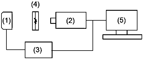
[0030] Specific implementation mode one: as figure 1 As shown, the infrared thermal imaging device for projective non-destructive detection of internal defects between film layers provided in this embodiment includes a flash light source 1, an infrared thermal imaging camera 2, a signal synchronization device 3, a tested part 4 and a computer 5, and a signal synchronization device 3 Connect with the flash light source 1 and the computer 5 respectively, the infrared thermal imager 2 is respectively connected with the computer 5 and the signal synchronization device 3, the detected part 4 is placed vertically between the infrared thermal imager 2 and the flash light source 1, and is connected with the infrared thermal image The lens of instrument 2 is parallel.

[0031] When the above detection device is in operation, the flash light source 1 instantly irradiates and heats the tested part 4 from the back of the tested part 4, and the temperature of the tested part 4 rises. Duri...

specific Embodiment approach 2

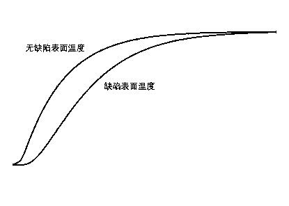
[0034] Specific implementation mode 2: This implementation mode provides a projective non-destructive infrared thermal imaging method for detecting internal defects between film layers, which is caused by the blockage of heat flow in the defective part of the multilayer film and the smooth passage of heat flow in the non-defective part when pulsed heating is used. The phenomenon of different surface temperatures identifies the location and size of the defect. The specific implementation steps are as follows:

[0035] 1. Preliminary calculation of the pulse time constant and pulse energy according to the thermal material characteristics of the multilayer film structure;

[0036] 2. Adjust the pulse time of the flash light source and the signal synchronization device;

[0037] 3. Place the tested part vertically in front of the thermal imaging camera to ensure that the tested part is parallel to the lens of the thermal imaging camera;

[0038] 4. The flash light source pulses ...

specific Embodiment approach 3

[0045] Specific implementation mode three: This implementation mode provides an infrared thermal imaging method for projection-type nondestructive detection of internal defects between film layers, and the specific implementation steps are as follows:

[0046] 1. Preparation of the inspected part: Electroplating on the substrate with Ni thin film and Cu film as the seed layer;

[0047] 2. Use a laser pulse with a spot diameter of 10mm and a wavelength of 808nm to heat the object to be tested, control the irradiation pulse time to 500μs, and the irradiation energy density to 20KJ / m 2 ;

[0048] 3. At the same time as the pulse heating, the infrared thermal imaging camera collects at least 5 pieces of temperature image data on the surface of the tested part within 1000μs of heating;

[0049] 4. Under the premise of sufficient cooling, steps 2 and 3 can be repeated many times, preferably 4 to 5 times;

[0050] 5. Use a computer to superimpose and calculate the collected tempera...


PUM

PropertyMeasurementUnit
thicknessaaaaaaaaaa
thicknessaaaaaaaaaa
thicknessaaaaaaaaaa

Abstract

The invention discloses a projection type infrared thermal imaging device and method for non-destructive detection of an internal defect between thin film layers. The device comprises a flashing light source, a thermal infrared imager, a signal synchronization device, a detected piece and a computer, wherein the signal synchronization device is connected with the flashing light source and the computer respectively; the thermal infrared imager is connected with the computer and the signal synchronization device; and the detected piece is perpendicularly placed between the thermal infrared imager and the flashing light source and parallel to a camera of the thermal infrared imager. According to the method, a defected portion and the size of the defected portion can be identified according to the phenomenon of different surface temperatures due to the fact that heat flow is blocked at the defected portion in multiple layers of thin films and successfully passes through a non-defected portion in the multiple layers of thin films during pulse heating excitation. The projection type infrared thermal imaging device has the characteristics of quickness, non-destructiveness, real-time performance and low detection cost; when the projection type infrared thermal imaging device is applied to the field of electronic information manufacturing such as microelectronics and microelectronics machinery, the manufacturing cost and the test cost can be substantially reduced, and the quality can be improved; and the projection type infrared thermal imaging device has a wide application prospect.

Description

technical field [0001] The invention belongs to the technical field of microelectronics and microelectronic machinery manufacturing, and relates to a novel defect detection device and method, in particular to a projection-type infrared thermal imaging device and method for nondestructive detection of internal defects between double-layer and multi-layer film layers. Background technique [0002] Multilayer thin film is the basic structure of thin film devices, microelectronic devices, microelectronic machinery (MEMS,) etc. in the field of information electronics manufacturing. It is characterized by double or multi-layer films and thin substrates made by evaporation, sputtering, chemical deposition, spin coating, bonding and other processes. During the preparation process, there will be tiny defects between the membrane and the membrane due to various reasons, such as air bubbles, delamination, cracks, slag inclusions, foreign matter and so on. In order to control the quali...

Claims


Application Information

Patent Timeline
Patent Type & Authority Patents(China)
IPC IPC(8): G01N25/72
CPCG01N25/72
Inventor 王晓婷王春青
Owner HARBIN INST OF TECH
Why Eureka
Try Eureka