Method and apparatus for efficiently implementing trace and/or logic analysis mechanisms on a processor chip

a logic analysis and processor chip technology, applied in the direction of detecting faulty computer hardware, error detection/correction, instruments, etc., can solve the problems of increasing the length of the debug phase, requiring a greater advanced lead time, and the design and development of digital logic circuits have become increasingly complex, so as to achieve the effect of reducing the design risk

Active Publication Date: 2006-05-23
HEWLETT-PACKARD ENTERPRISE DEV LP
View PDF4 Cites 6 Cited by
  • Summary
  • Abstract
  • Description
  • Claims
  • Application Information

AI Technical Summary

Benefits of technology

[0017]According to another aspect of the present invention, a processor includes an on-chip memory system, which includes at least one cache memory device accessed by a cache memory bus, which comprises an address path, a data path, and a control path. A multiplexer device selects which address, data and control signals will be routed to the cache memory set. When in a debug mode, the multiplexer selects address, data and control signals from the on-chip logic analyzer to store in the cache memory. Conversely, when the chip is operating in a normal mode, the multiplexer selects address, data and control signals from the CPU core to store in the cache memory. Other operating states may also be supported, such as an initialization mode, during which the multiplexer selects test logic as the source of address, data and control signals to store in the cache memory. Thus, by piggy-backing on the test port of the multiplexer, the on-chip logic analyzer has access to a memory bus and memory device that is as good as that which the CPU uses, without introducing any new dedicated memory devices into the chip layout, or any new timing considerations from the system perspective. Because the on-chip logic analyzer has access to a relatively large cache memory section (or sections) that are provided on the chip itself, the on-chip logic analyzer can store a relatively large quantity of state data, in an efficient manner, with a minimal design risk that the new hardware would interfere or prove incompatible with existing logic.

Problems solved by technology

The design and development of digital logic circuits has become increasingly complex, due in large measure to the ever-increasing functionality offered in such circuits.
As integrated circuits become more complex, the length of the debug phase increases, requiring a greater advanced lead-time before product release.
In addition, as the complexity of integrated circuits increase, it becomes necessary to fabricate more prototype iterations of the silicon (or “spins” of silicon) in order to remove successive layers of bugs from the design, thereby increasing the engineering and materials cost of the released product.
One of the chief difficulties encountered during the debug phase of a product is identifying the source of an error.
This can be extremely difficult because the error may make it impossible to obtain state information from the integrated circuit.
For example, in a processor, an error may cause the processor to quit executing, thus making it impossible to obtain the state data necessary to identify the source of the error.
Unfortunately, merely adding a soldered wire to a terminal or trace can create signal reflections, which may distort the data being monitored.
Thus, the manual probing of bus terminals and traces is impractical and inaccurate, especially those attached to high speed, highly complex chips.
More sophisticated techniques are also used, but are expensive and suffer, albeit to a lesser degree, from the same effects.
Both of these factors make it practically impossible to probe internal terminals of the chip or internal wire traces.
Moreover, to the extent that certain internal terminals and traces could be probed, the conventional methods for conducting such a probing operation are extremely expensive, and some might potentially corrupt the state of the terminals and traces being probed.
This approach, however, suffers in several respects.
Second, routing the desired state to external terminals often requires more wiring, silicon, drivers, pads and power than is affordable.
Attempts to do so can compromise the normal functioning of the chip.
And costs escalate throughout the design, often impacting the micropackaging and system board as well as the die.
Third, oftentimes the internal clock rate of the chip operates at a much higher rate than the external logic analyzers that receive and process the data.
The fastest commercial logic analyzers, despite their expense, are incapable of operating at GHz frequencies.
This solution, however, makes it more difficult to detect the bugs and errors that occur when the chip is running at full clock speeds.
The problem with this approach, however, is that it requires the allocation of a significant amount of chip space to incorporate such dedicated memory devices, and these memory devices, while used extensively during the design and development phase of the chip, add little or nothing to the performance of the chip once it is released into production.
Thus, the inclusion of dedicated memory space on the chip represents an opportunity cost, and means that functionality and / or performance is sacrificed to include this dedicated memory on the chip.
Consequently, the inclusion of memory for debug purposes, while helpful in the debug and test phase, is generally viewed as undesirable because of the accompanying loss of performance and functionality that must be sacrificed.
In relative terms, the largest dedicated on-chip memories typically are incapable of storing very much data.
Despite the apparent advantages that such a system would offer, to date no such system has been developed.

Method used


Image

  • Method and apparatus for efficiently implementing trace and/or logic analysis mechanisms on a processor chip
  • Method and apparatus for efficiently implementing trace and/or logic analysis mechanisms on a processor chip
  • Method and apparatus for efficiently implementing trace and/or logic analysis mechanisms on a processor chip

Examples


Embodiment Construction

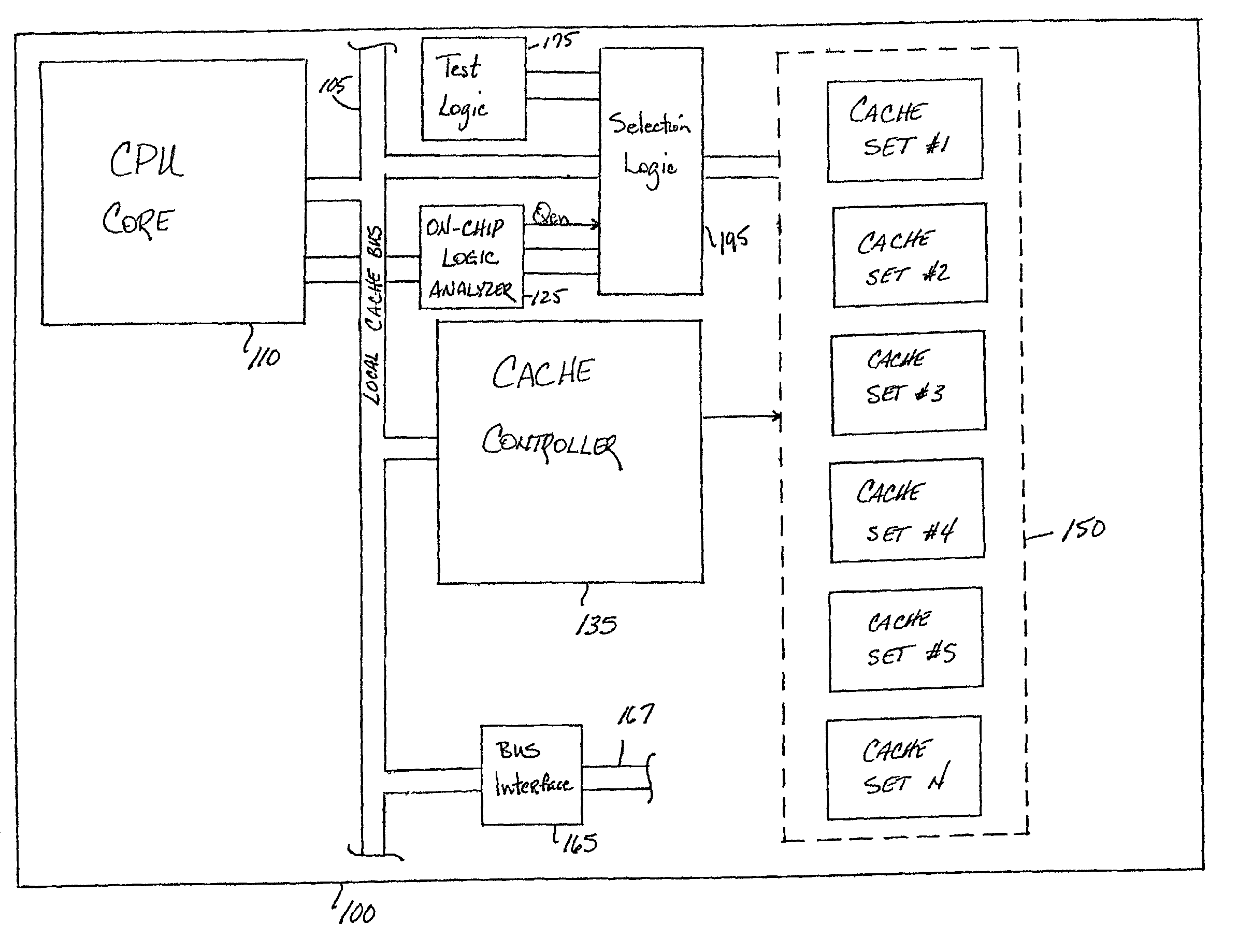
[0026]Referring initially to FIG. 1, the present invention constructed in accordance with the preferred embodiment generally comprises an integrated processor 100 that includes a CPU core 110 coupled to a cache memory 150. In accordance with normal convention, a cache controller 135 controls memory accesses to the cache memory 150. The CPU core 110, the cache controller 135 and the cache memory 150 preferably are coupled to a local cache bus 105. Other devices may also be coupled to the local cache bus 105, including a local bus interface 165 that interfaces the local cache bus 105 to a processor local bus 167. Various other devices may reside on the local bus 167, including an on-chip memory controller (not shown) that controls accesses to a system memory (not shown), and an on-chip I / O controller that controls accesses to both internal and external I / O devices. The processor 100 may be designed to operate in a multiple processor environment, and thus may be capable of transmitting...


PUM


Abstract

A system is disclosed in which an on-chip logic analyzer (OCLA) is included in an integrated circuit, such as a microprocessor. During debug modes, one or more sets of an on-chip cache memory are disabled from use by other circuitry in the integrated circuit, and reserved exclusively for use by the OCLA. Data stored in the reserved cache set can then be read out by the OCLA, and placed in a register that can be accessed by other logic internal or external to the integrated circuit. If the integrated circuit is operating under normal mode, the cache memory set can be used in conventional fashion by other circuitry with in the integrated circuit to enhance performance.

Description

CROSS-REFERENCE TO RELATED APPLICATIONS[0001]Method And Apparatus For Managing Timestamps When Storing Data, Ser No. 10 / 034,462, filed Dec. 28, 2001; An Efficient Word Recognizer For A Logic Analyzer Ser No. 10 / 034,227 filed Dec. 28, 2001; and Method And Apparatus For Implementing Loop Compression In A Program Counter Traces, Ser. No. 10 / 034,506, filed Dec. 28, 2001. now U.S. Pat. No. 6,691,207 B2 issued Feb. 10, 2004;all of which are incorporated by reference herein.STATEMENT REGARDING FEDERALLY SPONSORED RESEARCH OR DEVELOPMENT[0002]Not applicable.BACKGROUND OF THE INVENTION[0003]1. Field of the Invention[0004]The present invention relates generally to the design of digital logic devices. More specifically, the present invention relates to the design of digital logic devices, which include on-chip memory, to facilitate debugging and testing of such devices. Still, more particularly, the invention relates to an on-chip logic analyzer, which operates in conjunction with a portion of...

Claims


Application Information

Patent Timeline
Patent Type & Authority Patents(United States)
IPC IPC(8): G06F11/00G01R31/3177G06F11/25
CPCG06F11/25G01R31/3177
Inventor LITT, TIMOTHE
Owner HEWLETT-PACKARD ENTERPRISE DEV LP
Why Eureka
Try Eureka