
Methods of fabricating oxide layers by plasma nitridation and oxidation

a technology of oxide layer and plasma nitridation, which is applied in the direction of semiconductor devices, basic electric elements, electrical apparatus, etc., can solve the problems of deterioration of time dependent dielectric breakdown, increase in standby current, and disturbance of logic state, so as to improve the reliability of thick gate oxide layer and good electrical characteristics

Inactive Publication Date: 2006-05-30
SAMSUNG ELECTRONICS CO LTD
View PDF7 Cites 10 Cited by
  • Summary
  • Abstract
  • Description
  • Claims
  • Application Information

AI Technical Summary

Benefits of technology

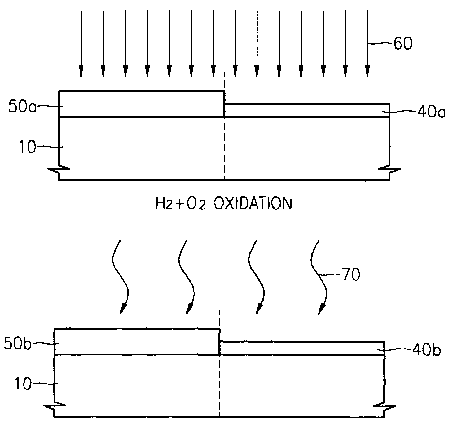
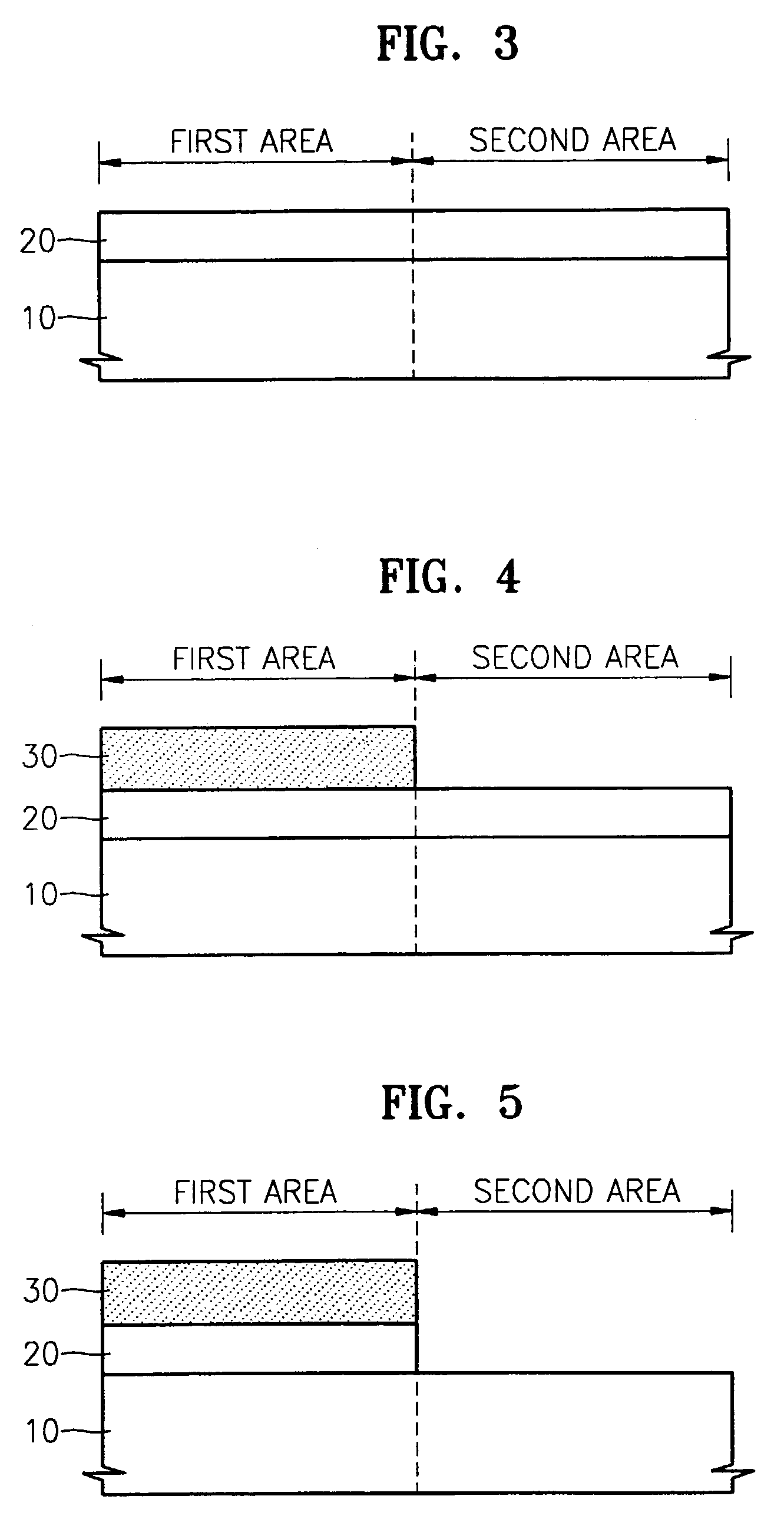
[0013]According to some embodiments of the present invention, there is provided a method of forming a gate oxide layer. Gate oxide layers having different thicknesses are formed on a substrate. The gate oxide layers having different thicknesses are subjected to plasma nitridation. The plasma nitridized gate oxide layers having different thicknesses are oxidized in an oxygen atmosphere containing hydrogen. Thus, in some embodiments, good electrical characteristics of a thin gate oxide layer of gate oxide layers having different thicknesses may be maintained and the reliability of a thick gate oxide layer may be improved.

Problems solved by technology

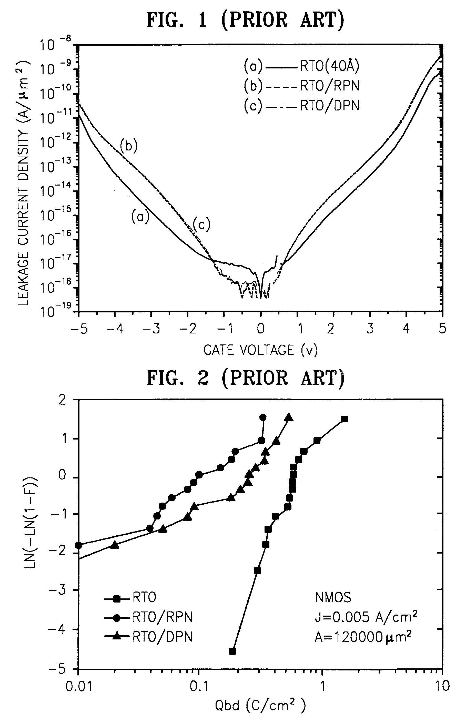
However, as the thickness of the gate oxide layers becomes thinner, a leakage current due to direct tunneling may increase, which may cause an increase in a standby current, the disturbance of a logic state, the deterioration of Time Dependent Dielectric Breakdown (TDDB) characteristics and / or other undesirable characteristics.
Thus, the reliability of the thick gate oxide layer may be very seriously deteriorated.
This appears to be because the electron trap sites are created due to silicon dangling bonds, bivalent nitrogen bonds and / or the like generated during plasma nitridation and then injected electrons are trapped in the electron trap sites, which may increase an intensity of a local electrical field, thereby causing a dielectric breakdown.
However, as shown in FIG. 2, the deterioration of the reliability of the thick gate oxide layer, represented by a reduction in the Qbd value, may not allow the application of plasma nitridation in the device, and thus may be very problematic.

Method used


Image

  • Methods of fabricating oxide layers by plasma nitridation and oxidation
  • Methods of fabricating oxide layers by plasma nitridation and oxidation
  • Methods of fabricating oxide layers by plasma nitridation and oxidation

Examples


Embodiment Construction

[0023]The present invention now will be described more fully hereinafter with reference to the accompanying drawings, in which embodiments of the invention are shown. However, this invention should not be construed as limited to the embodiments set forth herein. Rather, these embodiments are provided so that this disclosure will be thorough and complete, and will fully convey the scope of the invention to those skilled in the art. In the drawings, the thickness of layers and regions are exaggerated for clarity. Like numbers refer to like elements throughout. It will be understood that when an element such as a layer, region or substrate is referred to as being “on” or extending “onto” another element, it can be directly on or extend directly onto the other element or intervening elements may also be present. In contrast, when an element is referred to as being “directly on” or extending “directly onto” another element, there are no intervening elements present.

[0024]In methods of fo...


PUM

PropertyMeasurementUnit
temperatureaaaaaaaaaa
areaaaaaaaaaaa

Abstract

Oxide layers, including gate oxide layers having different thicknesses, are formed, plasma nitridized, and oxidized in an oxygen atmosphere containing hydrogen at a high temperature. Electron trap sites and stress occurring during plasma nitridation may be removed during oxidation.

Description

RELATED APPLICATION[0001]This application claims the benefit of Korean Patent Application No. 2002-0069661, filed Nov. 11, 2002, the disclosure of which is hereby incorporated herein by reference in its entirety as if set forth fully herein.FIELD OF THE INVENTION[0002]The present invention relates to methods of fabricating semiconductor devices, and more particularly to methods of forming oxide layers such as gate oxide layersBACKGROUND OF THE INVENTION[0003]With the growing diversity of semiconductor devices, the device characteristics also may become diverse. For example, devices in which logic devices or Central Processing Units (CPUs) are merged with Dynamic Random Access Memories (DRAMs) or Static Random Access Memories (SRAMs) are being developed and marketed. In such devices, gate oxide layers having different thicknesses may be formed within a single chip in order to maintain each of the characteristics of the merged devices. Thus, a dual gate oxide layer composed of two dif...

Claims


Application Information

Patent Timeline
Patent Type & Authority Patents(United States)
IPC IPC(8): H01L21/31H01L21/336H01L21/28H01L21/314H01L21/8234H01L29/51
CPCH01L21/28194H01L21/28202H01L21/3144H01L29/518H01L29/513H01L29/517H01L21/823462H01L21/02323H01L21/31H01L21/02332H01L21/0234
Inventor HYUN, SANG-JINHONG, SUG-HUNSHIN, YU-GYUN
Owner SAMSUNG ELECTRONICS CO LTD
Learn More