GaN group semiconductor light-emitting element with concave and convex structures on the substrate and a production method thereof

a technology of semiconductor light-emitting elements and concave and convex structures, which is applied in the manufacture of semiconductor/solid-state devices, semiconductor devices, electrical devices, etc., can solve the problems of affecting the efficiency of light-emitting layer external removal, affecting the efficiency of light-emitting, and posing a cost problem

Inactive Publication Date: 2006-05-30
TOYODA GOSEI CO LTD
View PDF23 Cites 130 Cited by
  • Summary
  • Abstract
  • Description
  • Claims
  • Application Information

AI Technical Summary

Problems solved by technology

In LED, an important issue is how efficiently the light produced in the light-emitting layer can be externally taken out (what is called, light-extraction efficiency).
However, cutting 4 facets of a small chip with an angle is a difficult processing, posing a problem in costs.
Furthermore, the light advancing in the vertical direction is also associated with problems in that a standing wave that repeats reflection between an interface of GaN group semiconductor layer / sapphire substrate and an interface of GaN group semiconductor layer / p-type electrode (or sealing material) is formed and the like, which in turn hinder light-extraction efficiency.
In addition to the problem of the light-extraction efficiency as mentioned above, the following problem of lower output is present when InGaN is used as a material of a light-emitting layer and the ultraviolet light is to be emitted.
However, the ELO method is problematic in that the methods for growing a GaN layer to be a base, forming a mask layer and re-growing are necessary, and growth in a number of times is necessary, thus increasing the number of steps.
In addition, because a re-growth interface exists, it has a problem that, although dislocation density reduces, the output does not increase easily.
It has been also found that, when a barrier layer is made thin in the quantum well structure, Mg is diffused from the p-type layer formed thereon to a light-emitting layer and forms a non-radiative center, thus problematically preventing high output of an ultraviolet light-emitting element.

Method used


Image

  • GaN group semiconductor light-emitting element with concave and convex structures on the substrate and a production method thereof
  • GaN group semiconductor light-emitting element with concave and convex structures on the substrate and a production method thereof
  • GaN group semiconductor light-emitting element with concave and convex structures on the substrate and a production method thereof

Examples


example 1

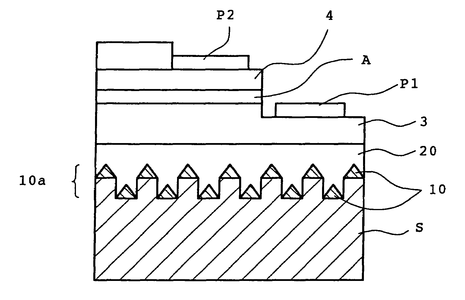
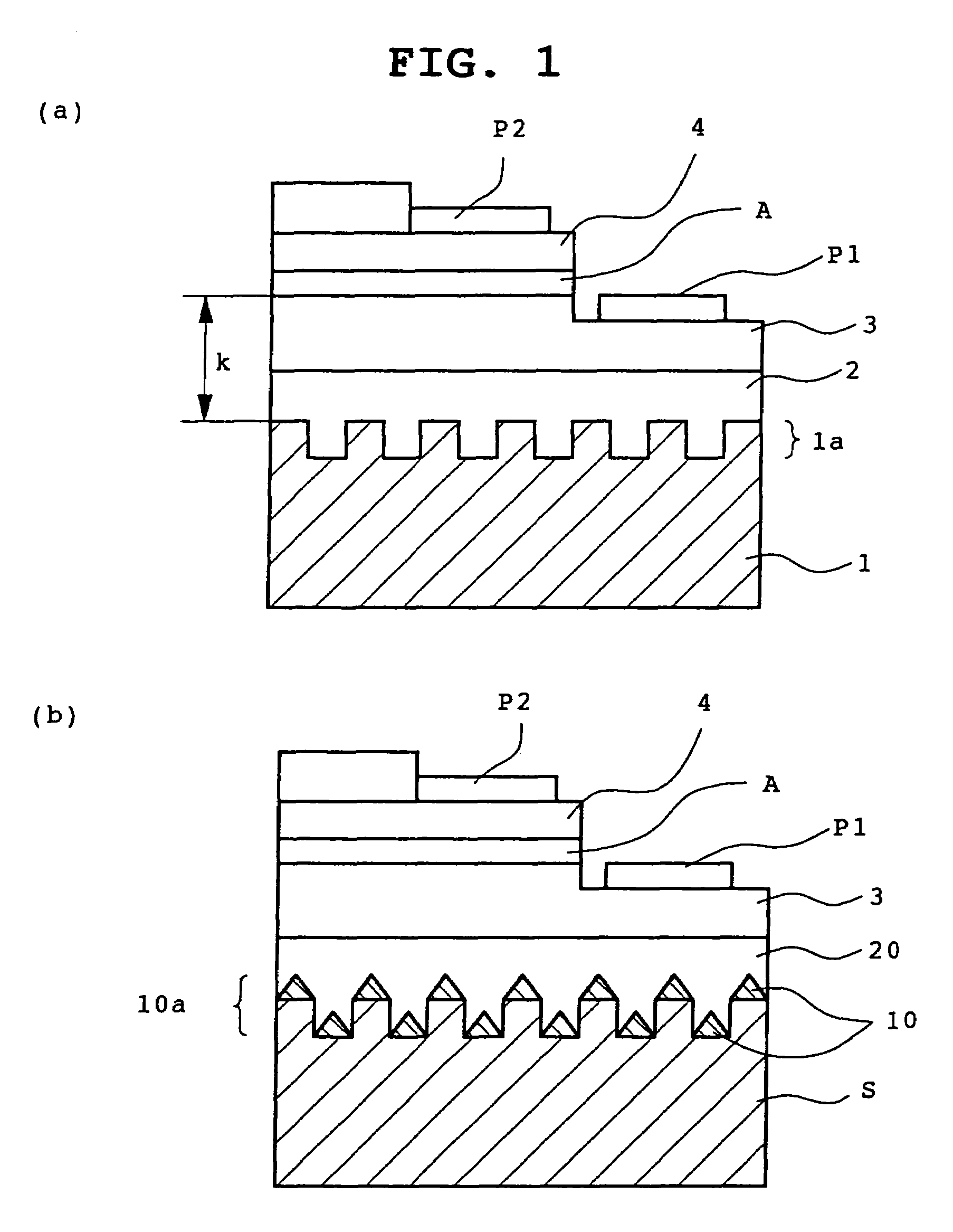
[0147]In this Example, concaves and convexes of a sapphire substrate were buried by said facet growth method according to the above-mentioned embodiment (I) to give a concavo-convex refractive index interface and a GaN group LED was actually prepared as shown in FIG. 1(a).

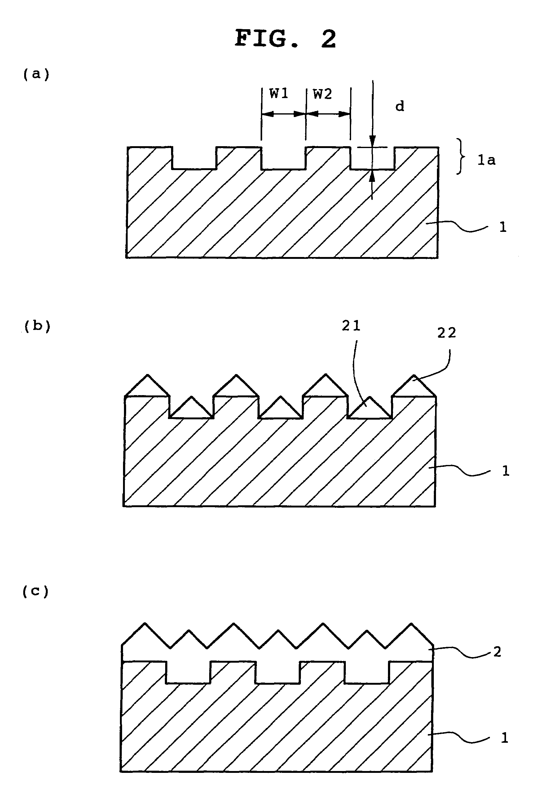
[0148]A stripe pattern (width 2 μm, period 4 μm, stripe orientation: the longitudinal direction of the stripe is direction for GaN group crystal grown on the substrate) was formed on a C-plane sapphire substrate using a photoresist, etched with an RIE apparatus until the cross section became a 2 μm deep square, whereby a substrate having a surface having concaves and convexes of a stripe pattern was obtained as shown in FIG. 2(a). The aspect ratio then of the cross section of the stripe groove was 1.

[0149]After removing the photoresist, the substrate was set on an MOVPE apparatus and the temperature was raised to 1100° C. under a gas atmosphere (main component nitrogen) to conduct thermal cleaning. The temperature...

example 2

[0162]In this Example, a concavo-convex facet structure comprising an AlGaN crystal was formed by said facet growth method according to the above-mentioned embodiment (II), as shown in FIG. 1(b), which was buried in GaN to give a concavo-convex refractive index interface, whereby a GaN group LED was actually prepared.

[0163]In completely the same manner as in Example 1, stripe patterned concaves and convexes were formed on a C-plane sapphire substrate, which was set on an MOVPE apparatus, and the temperature was raised to 1100° C. under a gas atmosphere (main component nitrogen) to conduct thermal cleaning. The temperature was lowered to 500° C. and TMG was flown as a III group starting material, and ammonia as an N starting material, whereby a GaN low temperature buffer layer having a thickness of 30 nm was grown.

[0164]Then the temperature was raised to 1000° C. and TMG and ammonia as starting materials, whereby a GaN layer was grown in about 100 nm. Then trimethylaluminum (TMA) was...

example 3

[0168]In this Example, a concavo-convex facet structure comprising a GaN crystal was formed by said facet growth method according to the above-mentioned embodiment (II), as shown in FIG. 4(c), which was covered with 50 pairs of Bragg reflective layers having an AlGaN / GaN superlattice structure to give a concavo-convex multi-layer refractive index interface, whereby a GaN group LED was actually prepared.

[0169]In completely the same manner as in Example 1, stripe patterned concaves and convexes were formed on a C-plane sapphire substrate, which was set on an MOVPE apparatus, and the temperature was raised to 1100° C. under a gas atmosphere (main component nitrogen) to conduct thermal cleaning. The temperature was lowered to 500° C. and TMG was flown as a III group starting material, and ammonia as an N starting material, whereby a GaN low temperature buffer layer having a thickness of 30 nm was grown.

[0170]Then the temperature was raised to 1000° C. and TMG and ammonia as starting mat...


PUM


Abstract

Concaves and convexes 1a are formed by processing the surface layer of a first layer 1, and second layer 2 having a different refractive index from the first layer is grown while burying the concaves and convexes (or first crystal 10 is grown as concaves and convexes on crystal layer S to be the base of the growth, and second crystal 20 is grown, which has a different refractive index from the first crystal). After forming these concavo-convex refractive index interfaces 1a (10a), an element structure, wherein semiconductor crystal layers containing a light-emitting layer A are laminated, is formed. As a result, the light in the lateral direction, which is generated in the light-emitting layer changes its direction by an influence of the concavo-convex refractive index interface and heads toward the outside. Particularly, when an ultraviolet light is to be emitted using InGaN as a material of a light-emitting layer, a quantum well structure is employed and all the layers between the quantum well structure and the low temperature buffer layer are formed of a GaN crystal, removing AlGaN. The quantum well structure preferably consists of a well layer made of InGaN and a barrier layer made of GaN, and the thickness of the barrier layer is preferably 6 nm–30 nm.

Description

TECHNICAL FIELD[0001]The present invention relates to a semiconductor light-emitting element (hereinafter to be also referred to simply as a light-emitting element). Particularly, this invention relates to a semiconductor light-emitting element having a light-emitting layer made of a GaN group semiconductor crystal (GaN group crystal).BACKGROUND ART[0002]The basic element structure of a light-emitting diode (LED) comprises a crystal substrate, and an n-type semiconductor layer, a light-emitting layer (including DH structure, MQW structure, SQW structure) and a p-type semiconductor layer sequentially grown thereon, wherein each of the n-type layer, the conductive crystal substrate (SiC substrate, GaN substrate and the like) and the p-type layer has an external outlet electrode.[0003]For example, FIG. 8 shows one exemplary constitution of an element (GaN group LED) comprising a GaN group semiconductor as a material of a light-emitting layer, wherein a GaN group crystal layer (n-type G...

Claims


Application Information

Patent Timeline
Patent Type & Authority Patents(United States)
IPC IPC(8): H01L29/22H01L29/227H01L29/24H01L33/12H01L33/22H01L33/32
CPCH01L33/22H01L33/12H01L33/32
Inventor TADATOMO, KAZUYUKIOKAGAWA, HIROAKIOUCHI, YOICHIROTSUNEKAWA, TAKASHI
Owner TOYODA GOSEI CO LTD
Why Eureka
Try Eureka