Contact grid array system

Active Publication Date: 2006-06-06
NEOCONIX INC
View PDF125 Cites 43 Cited by
  • Summary
  • Abstract
  • Description
  • Claims
  • Application Information

AI Technical Summary

Benefits of technology

[0040]For even higher density interconnections, additional parallel circuit elements may be stacked and electrically connected through additional BLGA connectors to create a three-dimensional package. A retentive force is not inherent, as with pin-and-socket-type interconnections, but a clamping mechanism is needed to create the force necessary to ensure each contact member is compressed an appropriate amount during engagement. This is needed to form the required interconnections to the circuit elements. Thermal management structures and other electrical circuitry may be included within the structure to enhance overall system performance.
[0041]PCB techniques are used to

Problems solved by technology

The microfabrication techniques disclosed by Khoury et al. have inherent and practical limitations with resp

Method used


Image

  • Contact grid array system
  • Contact grid array system
  • Contact grid array system

Examples


Example

[0079]For purposes of brevity and clarity, like components and elements of the apparatus of this invention will bear the same designations or numbering throughout the figures.

DESCRIPTION OF THE PREFERRED EMBODIMENT

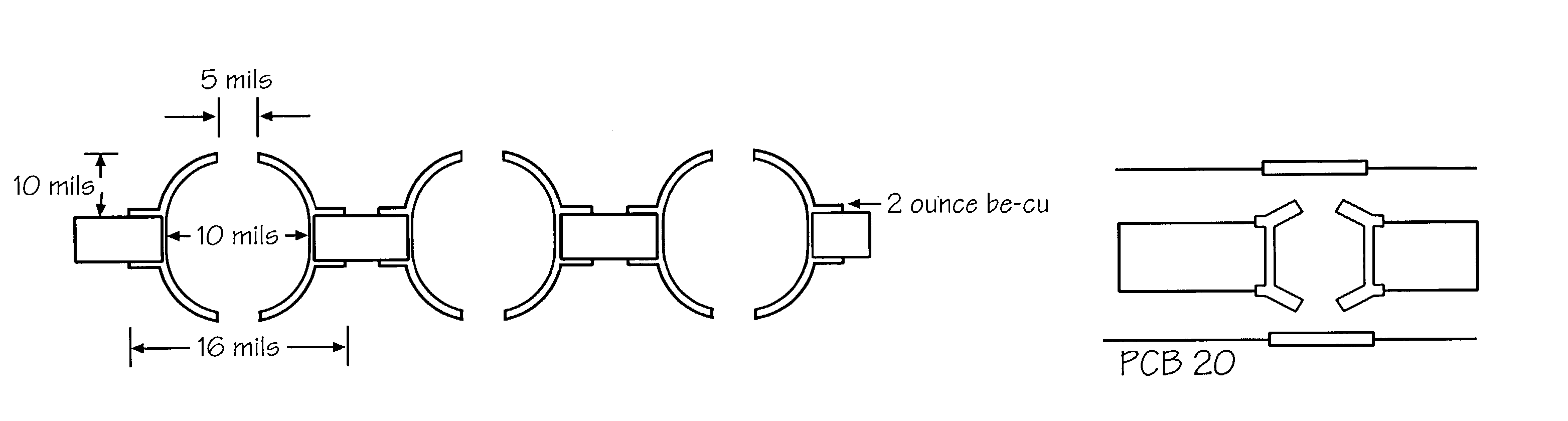
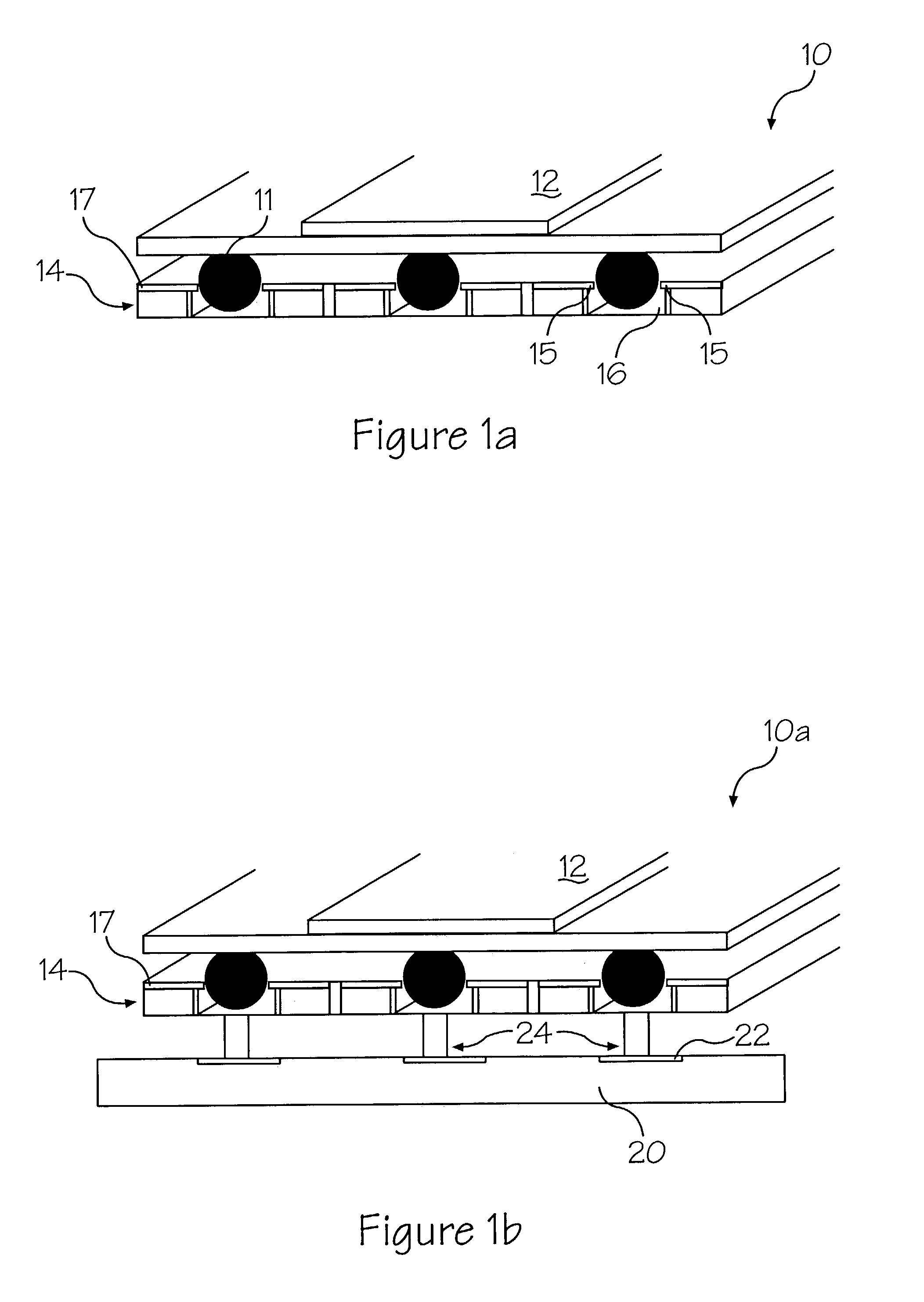
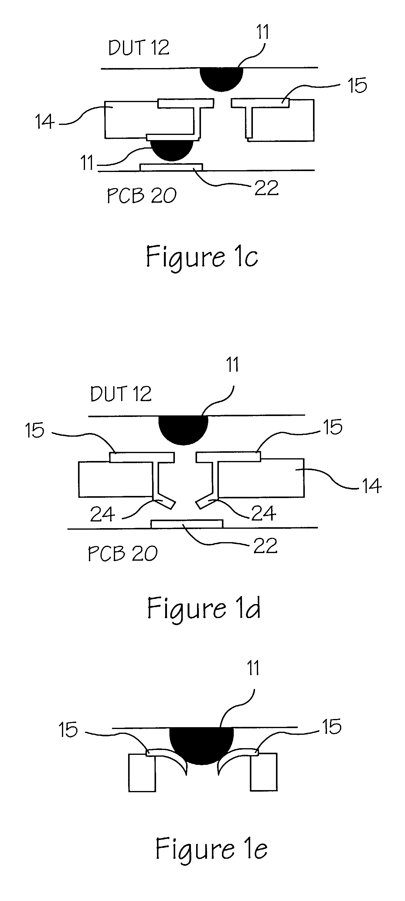
[0080]Generally speaking, the invention features a scalable, low cost, reliable, compliant, low profile, low insertion force, high-density, separable and reconnectable electrical connection for high speed, high performance electronic circuitry and semiconductors. The electrical connection can be used, for example, to make electrical connections from one PCB to another PCB, MPU, NPU, or other semiconductor device.

[0081]The invention comprises a connection system consisting of a beam land grid array (BLGA) or a ball beam grid array (BBGA). The electrical and mechanical functionality of the BLGA and / or BBGA lends itself to numerous applications in the electronics space. It allows for short interconnections to be established between almost any electrical contact surfaces, thus...


PUM


Abstract

A scalable, low cost, reliable, compliant, low profile, low insertion force, high-density, separable and reconnectable electrical connection for high speed, high performance electronic circuitry and semiconductors. The electrical connection can be used to make, for example, electrical connections from one Printed Circuit Board (PCB) to another PCB, MPU, NPU, or other semiconductor device.

Description

FIELD OF THE INVENTION[0001]The invention pertains to separable electronic contact systems and, more particularly, to a separable electronic contact grid array system having exceptional elasticity and low inductance properties, and which is elastically and electrically functional across the entire gap separating the electronic devices to be connected.BACKGROUND OF THE INVENTION[0002]The ability to make separable electrical contact with contacts of miniature electronic circuits has become more problematic as the mechanical, electrical, and reliability requirements of these electrical contacts become more demanding. Nano springs, pogo pins, micro springs, and other miniature contact devices have been developed to deal with the problem of making reliable electrical contact between a microcircuit and the rest of an electronic system. The problem for the industry, however, is that no particular contact design appears to provide all of the properties required, even where specially designe...

Claims


Application Information

Patent Timeline
IPC IPC(8): H01R12/00
CPCH05K3/4092H01R12/52H01L2924/14H01L2924/19041H05K3/202H05K3/326H05K3/42H01L2924/10253H05K2201/0397H05K2201/10378H01L2924/00
Inventor WILLIAMS, JOHN D.
Owner NEOCONIX INC
Why Eureka
Try Eureka