
Solder bar for high power flip chips

a flip chip and solder bar technology, applied in the field of flip chip integrated circuits, can solve the problems of typical flip chip solder bumps experiencing early failures, functional and reliability problems during the device operating life, and limited area in which to position the solder bumps, so as to reduce the current density of solder. the effect of increasing the cross-sectional area

Inactive Publication Date: 2006-06-06
FLIPCHIP INT
View PDF16 Cites 26 Cited by
  • Summary
  • Abstract
  • Description
  • Claims
  • Application Information

AI Technical Summary

Benefits of technology

[0015]Briefly described, and in accordance with a preferred embodiment thereof, the present invention is a solder bar formed upon the upper surface of a flip chip integrated circuit or other “first substrate”. The solder bar of the present invention is adapted to join a first electrical contact on the first substrate to a second electrical contact on a second substrate. This solder bar replaces one or more discrete solder bumps to effectively increase the cross-sectional area of the solder interconnect, thereby reducing the current density in the solder. The solder bar includes first and second generally circular solder pads that are formed upon the upper surface of the first substrate; these solder pads may be patterned “under bump metal” (UBM) layers. Each of the first and second generally circular solder pads has a predetermined diameter D, and the centers of such first and second generally circular solder pads are spaced apart from each other by a spacing distance, or bar length, BL. A solder bar pad is also formed upon the upper surface of the first substrate having a bar width BW and connecting the first and second generally circular solder pads to each other said second circular solder pad; bar width BW is less than the diameter D of the first and second generally circular solder pads.

Problems solved by technology

However, the need for conducting relatively high currents, particularly power and ground interconnections, through such solder bumps in high power applications poses a problem relating to solder and UBM (Under Bump Metal) electromigration, which can in turn present functional and reliability issues during the device operating life.
Typical flip chip solder bumps can experience early failures due to electromigration when exposed to a high current density at a given junction temperature.
However, in a given flip chip design, there is typically a limited amount of area in which to position the solder bumps, even in a full-array type design.
There are limits as to how close together such solder bumps can be arranged to avoid the violation of processing design rules, and the use of two or more solder bumps to form parallel connections is not a very effective use of the limited area available in which to make all necessary electrical interconnections.
Another method of handling large currents is to use wire bonds instead of solder bumps, but this approach is not cost effective; it tends to increase the size of the integrated circuit die, and may not meet the inductance requirements of the application.

Method used


Image

  • Solder bar for high power flip chips
  • Solder bar for high power flip chips
  • Solder bar for high power flip chips

Examples


Embodiment Construction

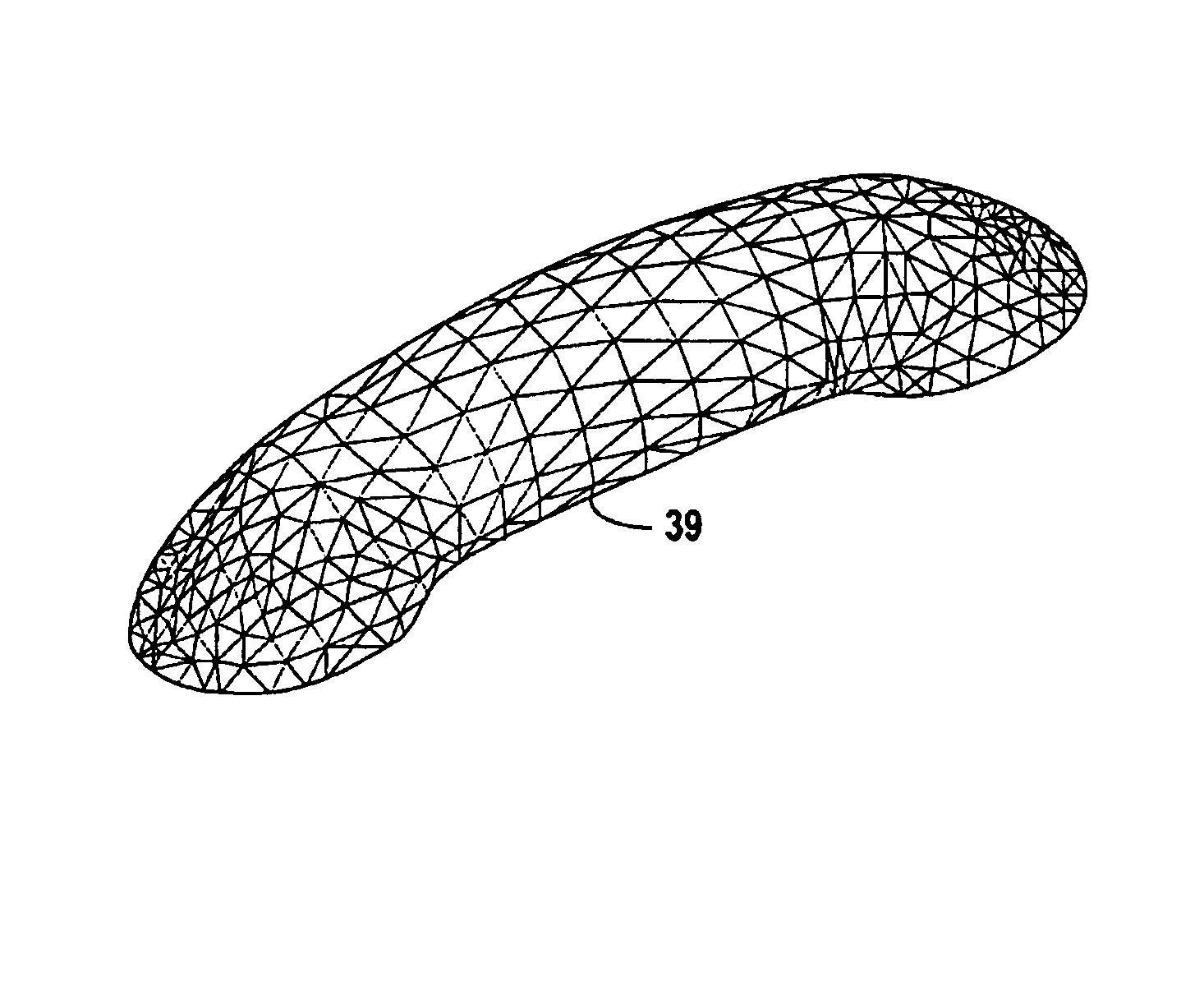
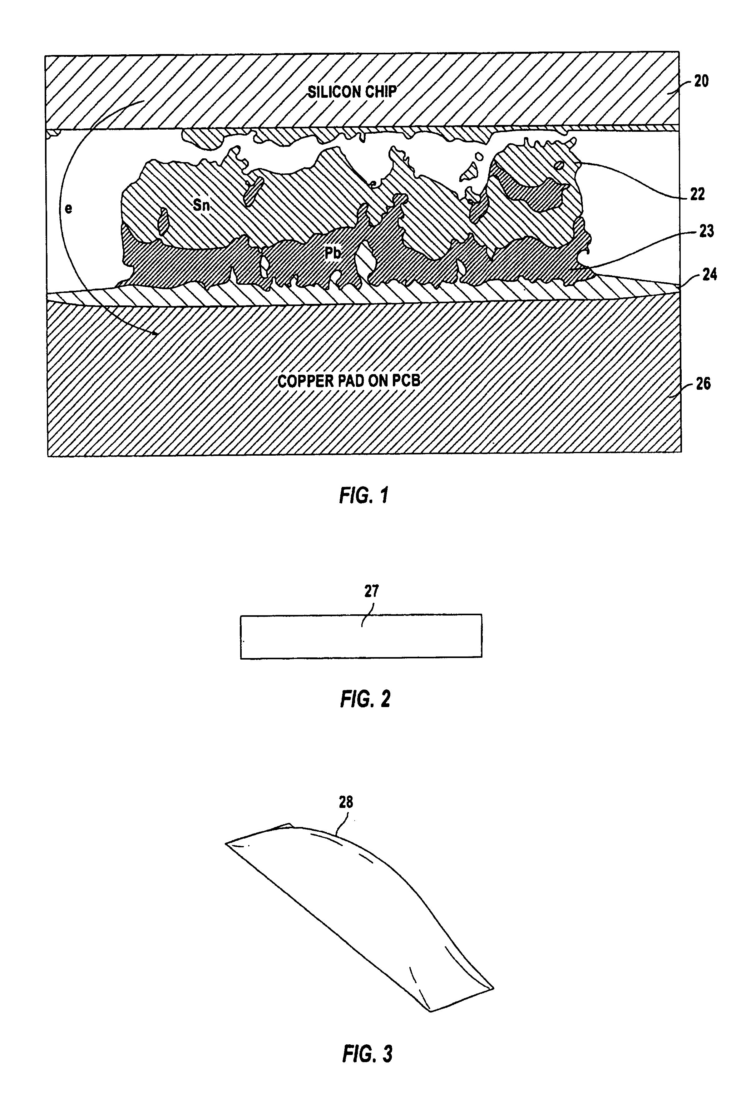
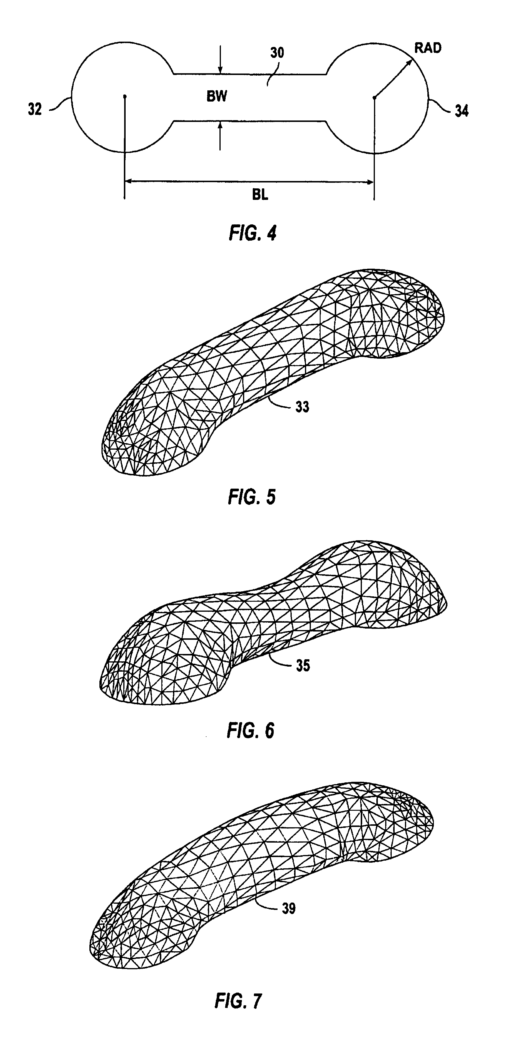
[0039]Before describing the preferred embodiment of the present invention, it may be helpful to first consider a very basic, non-optimal structure for a solder bar. A simple rectangular UBM (Under Bump Metal) structure 27 for a solder bar is shown in FIG. 2. In order to predict the results of using such a configuration, a computer software model was used. One such computer model known by the name “Surface Evolver” is available from the University of Minnesota Geometry Center, and can be downloaded over the Internet via a Web page having the domain name “http: / / geom.umn.edu / software / download / evolver.html”. Using the rectangular layout shown in FIG. 2, and based upon the selection of a particular solder bar volume VB, the Surface Evolver computer model results in a non-optimal solder bar profile 28 shown in FIG. 3. This simple solder bar structure does not achieve the desired results, as the height of solder bar 28 is continuously changing over its length. When this type of solder bar...


PUM


Abstract

A solder bar compatible with conventional flip chip technology fabrication methods for high power / high current applications includes first and second generally circular solder pads of diameter D formed upon a substrate and connected by a solder bar pad of width BW. The centers of the generally circular solder pads are spaced apart by distance BL (bar length). A mass of solder having volume VB is formed over the first and second generally circular solder pads and over the solder bar pad to form a dog-bone shaped solder bar. The solder bar reaches height H1 above the centers of the first and second generally circular solder pads, and reaching height H2 above the midpoint of the solder bar pad. The values for diameter D, bar length BL, bar width BW, and solder volume VB are selected in such manner that H1 and H2 are approximately equal. Conventional circular (as viewed from above) solder bumps can be formed upon the same substrate; in this case, heights H1 and H2 are made approximately equal to the height of the conventional solder bumps.

Description

BACKGROUND OF THE INVENTION[0001]1. Field of the Invention[0002]The present invention relates generally to flip chip integrated circuits, and more particularly, to flip chip type solder joints capable of carrying greater currents at lower current densities.[0003]2. Description of the Relevant Art[0004]Flip chip surface mount technology is well known in the semiconductor industry for simplifying the packaging and interconnection of integrated circuits. Typically, a series of circular (as viewed from above, or semi-spherical in three dimensions) solder bumps are formed upon the upper surface of an integrated circuit or other substrate in electrical contact with active or passive devices formed upon such substrate. Such solder bumps are then aligned with pads formed upon a second substrate to which the first substrate is to be mounted. The use of solder bumps to interconnect such flip chip integrated circuits to underlying support substrates is disclosed, for example, within U.S. Pat. ...

Claims


Application Information

Patent Timeline
IPC IPC(8): H01L23/48H01L23/52H01L29/40H01L21/48H01L23/498H01L23/538H05K3/34
CPCH01L21/4853H01L23/49838H01L23/5386H01L23/49816H01L2224/0401H05K3/341H05K3/3436H01L2224/05552H01L2224/14051H01L2224/13012H01L2924/10253H01L2924/01327H01L2924/01322H01L2924/00H01L2924/00012
Inventor ELENIUS, PETERYANG, HONG
Owner FLIPCHIP INT
Learn More