Electronic ballast

a technology of electronic ballast and electronic ballast, which is applied in the direction of electric variable regulation, process and machine control, instruments, etc., can solve the problems of large bus capacitors, more expensive, and occupying more area on printed circuit boards

Inactive Publication Date: 2006-06-13
LUTRON TECH CO LLC
View PDF12 Cites 71 Cited by
  • Summary
  • Abstract
  • Description
  • Claims
  • Application Information

AI Technical Summary

Benefits of technology

[0013]In a preferred embodiment of the ballast, the energy storage element of the valley-fill circuit includes a bus capacitor that stores energy during a first predetermined charging portion of each half-cycle of the AC mains voltage, and delivers energy to the gas discharge lamp during a second predetermined discharge portion of each half-cycle of the AC mains voltage. The switched impedance of the valley-fill circuit includes a resistor in series with a controllably conductive device (a field effect transistor), through which the bus capacitor is charged.
[0014]In an alternative embodiment, the energy storage device of the valley-fill circuit includes a bus capacitor, and the switched impedance includes a buck inductor in series with a field effect transistor, connected together in a buck converter configuration. The bus capacitor stores energy during a first predetermined charging portion of each half-cycle of the AC mains voltage, and delivers energy to the gas discharge lamp during a second predetermined discharge portion of each half-cycle of the AC mains voltage. The buck inductor stores energy in response to conduction of the field effect transistor during the charging period of the bus capacitor, and transfers the stored energy to the bus cap

Problems solved by technology

However, using a relatively large bus capacitor to minimize ripple on the DC bus voltage comes with its disadvantages.
The bus capacitor must be fairly large, and is therefore more expensive and consumes more area on a printed circuit board, or the like, and volume within the ballast.
This results in the typical prior art ballast having a tendency to draw a relatively large amount of current during the time that the bus capacitor is charging, as shown in FIG. 1.
Consequently, this results in a distorted input current waveform giving rise to unwanted harmonic

Method used


Image

  • Electronic ballast
  • Electronic ballast
  • Electronic ballast

Examples


first embodiment

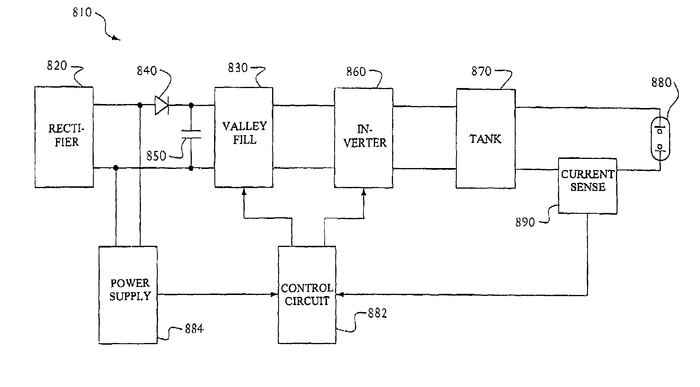
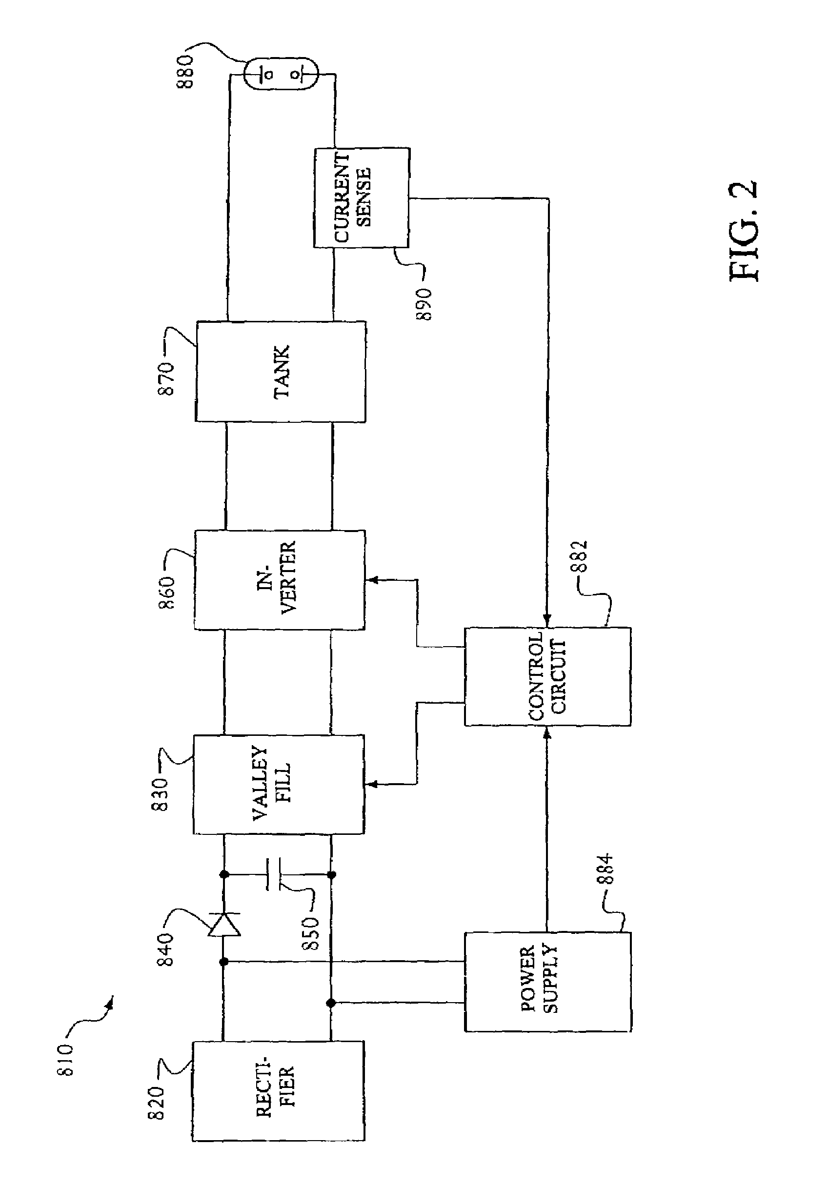
[0077]The control circuit 882 will be described with reference to FIGS. 20, 21, and 22. the control circuit 882 generates output drive signals to control the conduction of the switching devices 2112 and 924. The control circuit 882 receives as an input the half-wave rectified voltage from the current sense circuit 2240 and generates a DC voltage that represents actual light output from the lamps. This DC voltage, representative of light output, is compared to a reference voltage, indicative of a desired light level, to adjust the duty cycles of the switching devices 2112, 924 so as to minimize the difference between the light output voltage and the reference voltage. In a dimming electronic ballast, the reference voltage may be provided by an external input such as a 0-to-10 Volt control signal. Alternatively, the reference voltage may be generated by detecting a phase angle control signal applied to the ballast by means of the AC line voltage. In yet another embodiment, the referen...

second embodiment

[0089]the feedback circuit 2440 of FIG. 20 is shown in FIG. 24 and includes a microcontroller 26102 coupled to receive as inputs representative of the desired light level and the lamp current, and produce as outputs signals for driving the gates of the inverter switches. One such microcontroller suitable for use is manufactured by Motorola Corporation under the model number MC68HC08. For simplicity, analog-to-digital and digital-to-analog circuits necessary for interfacing the microcontroller 26102 with the analog circuitry of the ballast are considered to be within the ordinary skill of the art and are not shown here.

third embodiment

[0090]the feedback circuit 2440 of FIG. 20 is shown in FIG. 25 and includes in addition to the microcontroller 26102 a gate driver circuit 26104 that receives a single gate drive signal from the microcontroller 26102 and produces signals capable of controlling the operation of the inverter switches. One such gate driver circuit suitable for use is manufactured by International Rectifier under the part number IR2111. Of course, other suitable microcontrollers (such as a PIC16C54A from Power Integrations) and gate drivers may be substituted for the specific embodiments mentioned here. In addition, an application specific integrated circuit (ASIC) (not shown) may be substituted to provide the same functionality as the microcontrollers disclosed herein.

[0091]A high-level flowchart illustrating the operation of the feedback control circuit embodiment of FIGS. 24 and 25, shown in FIG. 26, includes the steps of measuring the lamp current IL (step 26110), and measuring the dimming signal VD...


PUM


Abstract

An electronic ballast for driving a gas discharge lamp includes a rectifier, a valley-fill circuit, an inverter having first and second series-connected controllably conductive switches having complementary duty cycles, a control circuit for controlling the controllably conductive switches, and an independent cat ear power supply to provide power to the ballast control circuits. The result is a ballast having substantially improved power factor, THD, and current crest factor. In a preferred embodiment, the valley-fill circuit includes an energy storage device that stores energy in response to a controllably conductive switch. In an especially preferred embodiment, the controllably conductive switch of the valley-fill circuit is also one of the switches of the inverter.

Description

CROSS REFERENCE TO RELATED APPLICATIONS[0001]This application is a continuation of U.S. patent application Ser. No. 09 / 887,848, filed Jun. 22, 2001 now abandoned by Robert S. Newman, Jr., et al. entitled “ELECTRONIC BALLAST” which is assigned to the assignee herein and the entire disclosure of which is hereby incorporated by reference herein.FIELD OF THE INVENTION[0002]The present invention relates to electronic ballasts and, more particularly, to electronic dimming ballasts for gas discharge lamps, such as fluorescent lamps.BACKGROUND OF THE INVENTION[0003]Electronic ballasts for fluorescent lamps typically can be analyzed as comprising a “front end” and a “back end”. The front end typically includes a rectifier for changing alternating current (AC) mains line voltage to a direct current (DC) bus voltage and a filter circuit for filtering the DC bus voltage. Electronic ballasts also often use a boost circuit for boosting the magnitude of the DC bus voltage. The filter circuit typic...

Claims


Application Information

Patent Timeline
IPC IPC(8): H05B37/00H05B41/28H05B41/282
CPCH05B41/28H05B41/282Y02B20/183Y02B20/00
Inventor NEWMAN, JR., ROBERT C.DEJONGE, STUARTTAIPALE, MARKTRAVAGLINI, DOMINICKSPIRA, JOEL S.
Owner LUTRON TECH CO LLC
Why Eureka
Try Eureka