Piezoelectric actuator, method for manufacturing the same, ink jet head, and ink jet recording apparatus
- Summary
- Abstract
- Description
- Claims
- Application Information
AI Technical Summary
Benefits of technology
Problems solved by technology
Method used
Image
Examples
embodiment 1
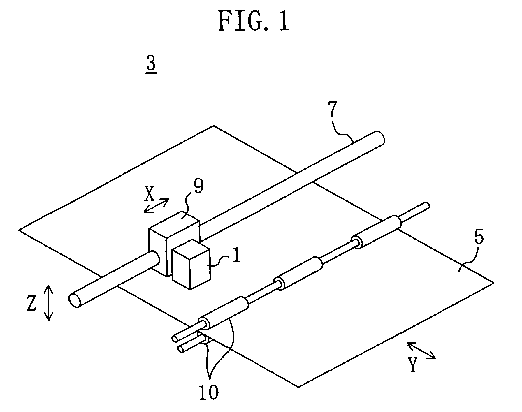
[0047]As illustrated in FIG. 1, an ink jet head 1 of the present embodiment is used in an ink jet printer 3, which is an ink jet recording apparatus. Ink droplets are discharged from the ink jet head 1 and land on a recording medium 5 such as paper, thereby recording information thereon.
[0048]The ink jet head 1 is mounted on a carriage 9 reciprocating along a carriage shaft 7 and is reciprocated in the primary scanning direction X along with the carriage 9. A pair of rollers 10 are provided for transferring the recording medium 5 in the secondary scanning direction Y by a predetermined amount after each iteration of the scanning movement of the carriage 9 in the primary scanning direction X.
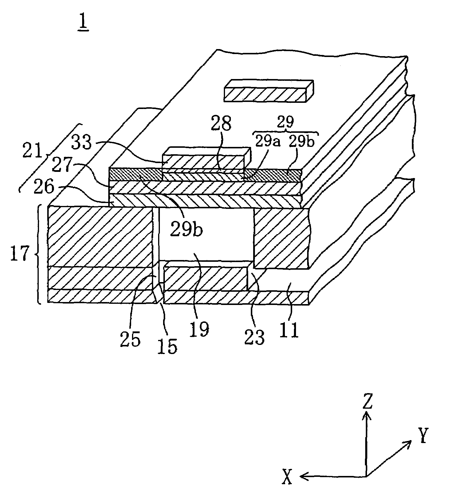
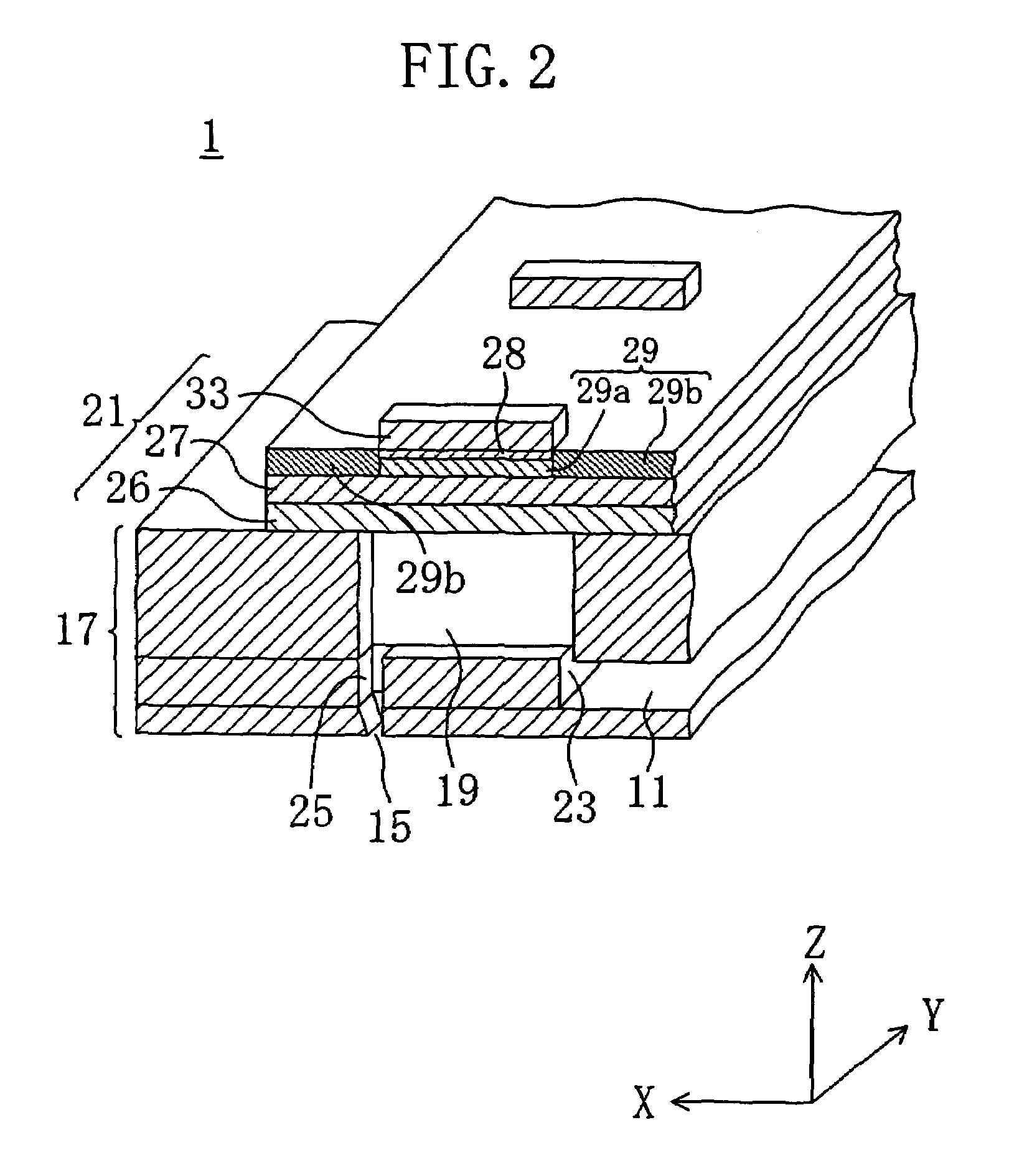
[0049]As illustrated in FIG. 2, the ink jet head 1 includes a head assembly 17 in which a common ink chamber 11, a plurality of pressure chambers 19 and a plurality of nozzles 15 are formed, and piezoelectric actuators 21 for applying a pressure on ink in the pressure chambers 19.
[0050]In the hea...
embodiment 2
[0077]A piezoelectric actuator of the present embodiment has substantially the same structure as that of the piezoelectric actuator of Embodiment 1, except that the crystal control layer is formed on the upper electrode after separating the upper electrode. The piezoelectric actuator of the present embodiment will now be described while focusing on what is different from Embodiment 1.
[0078]As illustrated in FIG. 9, the piezoelectric actuator 21 includes the vibration plate 26 made of Cr and having a thickness of 2 μm, the common electrode 27 made of Cu and having a thickness of 5.5 μm, which is formed on the vibration plate 26, the piezoelectric element 29 made of Pb(Zr,Ti)O3 and having a thickness of 3 μm, which is formed on the common electrode 27, the crystal control layer 28 made of lead lanthanum titanate and having a thickness of 0.05 μm, which is formed on the piezoelectric element 29, the separate electrode 33 made of Pt and having a thickness of 0.2 μm, which is formed on t...
embodiment 3
[0090]A piezoelectric actuator of the present embodiment has substantially the same structure as that of the piezoelectric actuator of Embodiment 1, except that it is manufactured by a so-called “direct process”. The piezoelectric actuator of the present embodiment will now be described while focusing on what is different from Embodiment 1.
[0091]As illustrated in FIG. 12, the piezoelectric actuator 21 includes the vibration plate 26 made of Cr and having a thickness of 2 μm, the common electrode 27 made of Cu and having a thickness of 5.5 μm, which is formed on the vibration plate 26, an adhesive layer 32 made of Ti and having a thickness of 50 nm, which is formed on the common electrode 27, an orientation control layer 36 made of a Pt—Ti alloy and having a thickness of 0.2 μm, which is formed on the adhesive layer 32, the crystal control layer 28 made of lead lanthanum titanate and having a thickness of 50 nm, which is formed on the orientation control layer 36, the piezoelectric e...
PUM
 Abstract
Description
Claims
Application Information


