Automated selection and placement of memory during design of an integrated circuit

a technology of automatic selection and placement of memory, applied in the direction of cad circuit design, program control, instruments, etc., can solve the problems of increasing complexity of integrated circuits and chips, increasing the difficulty of specifying and designing chips that perform as actually specified, and increasing the speed and capacity of chips

Inactive Publication Date: 2006-06-27
BELL SEMICON LLC
View PDF18 Cites 42 Cited by
  • Summary
  • Abstract
  • Description
  • Claims
  • Application Information

AI Technical Summary

Benefits of technology

[0013]Objects, features, and advantages of the invention may further be realized by a method of generating memory designs for an integrated circuit, comprising the steps of: inputting available memory resources into a memory resource database; inputting a request for at least one memory; selecting possible memory resources from the available memory resources to satisfy the request. The method would further consider

Problems solved by technology

Integrated circuits and chips have become increasingly complex, with the speed and capacity of chips doubling about every eighteen months.
The increased density of transistors per square centimeter and faster clock speeds, however, make it increasingly difficult to specify and design chips that perform as actually specified.
Unanticipated and sometimes subtle interactions between the transistors and other electronic structures may adversely affect the performance of the circuit.
These difficulties increase the expense and risk of designing and fabricating chips, especially those that are custom designed for a specific application.
The demand for complex custom-designed chips increases with the burgeoning number and variety of applications and products controlled by microprocessors yet the time and money required to design chips have become a bottleneck in bringing these products to market.
Without an assured successful outcome within a specified time, the risks have risen along with costs, and the result is that fewer organizations are willing to attempt the design and manufacture of custom chips.
The design of integrated circuits and the placement of the blocks has been a tedious and specialized engineering task.
For instance, an application-specific standard product (ASSP) such as of

Method used


Image

  • Automated selection and placement of memory during design of an integrated circuit
  • Automated selection and placement of memory during design of an integrated circuit
  • Automated selection and placement of memory during design of an integrated circuit

Examples


Embodiment Construction

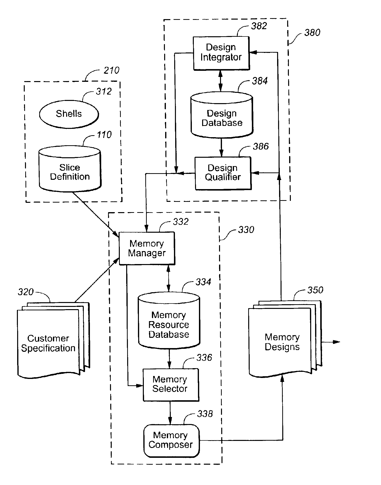
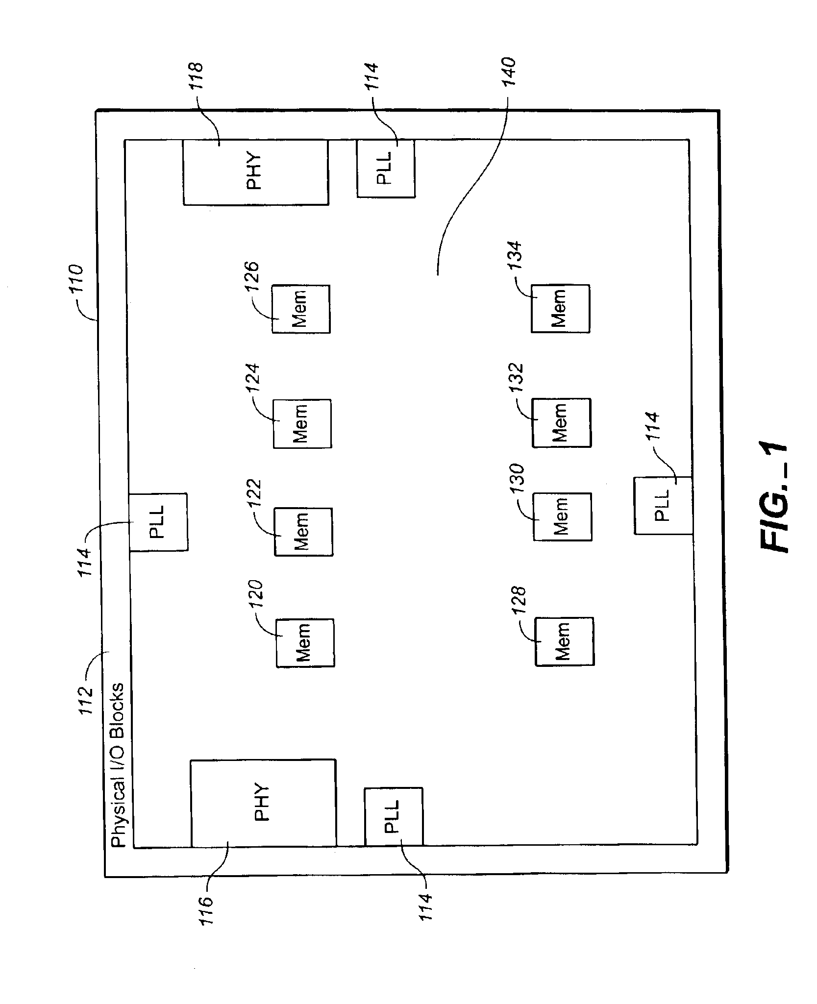
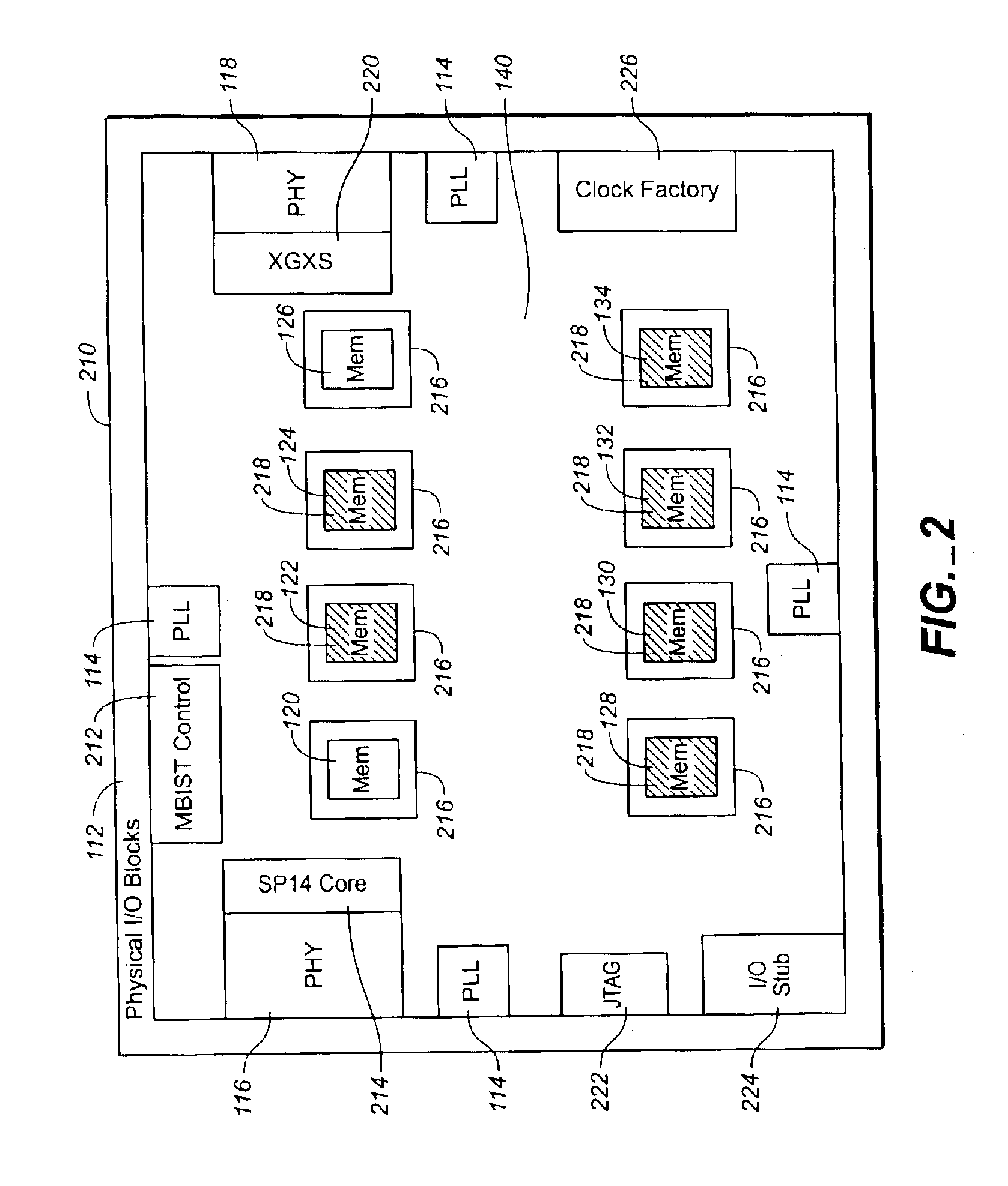
[0020]What is envisioned and disclosed herein is a computer hardware design tool installed on a computer system for designing, allocating, and integrating memory blocks on integrated circuits, also referred to as chips. The context for the design tool disclosed herein is to use a semiconductor slice having an embedded array of gate logic and having preestablished diffused memories distributed on the slice. The computer system upon which the design tool is installed may comprise any number of networked computers or a stand alone system, as is known in the art. Each computer system, moreover, may have one or more general-purpose programmable processors, executing instructions stored in memory, and may have one or more communications buses to support the transfer of data, commands and other information within and without the computer system.

[0021]The computer system has an operating system and one or more applications, preferably the integrated chip development tool as described herein...


PUM


Abstract

A tool for designing integrated circuits that optimizes the placement and timing of memory blocks within the circuit. Given a manufactured slice that has a number of blocks already diffused and logically integrated, the memory generation tool herein automatically considers the available diffused memory and the gate array of the slices to configure and optimize them into a customer's requirements for memory. The memory generation tool has a memory manager, a memory resource database, a memory resource selector, and a memory composer. Together these all interact to generate memories from the available memories within the memory resource database. The memory composer actually generates the RTL logic shells for the memories, and outputs the memory designs in Verilog, VHDL, or other tool synthesis language. Once a memory is created, it is tested. Upon successful testing, the memory manager updates the memory resource database to indicate the successfully tested memory is no longer available as a resource for the generation of further memories. A design integrator may review the memory designs output and further integrate the memory, its timing, testing, etc. with other blocks and functions of the integrated circuit.

Description

CROSS REFERENCE TO RELATED APPLICATIONS[0001]The present application is related to the following United States Patent Applications, which are hereby incorporated by reference in their entireties: copending U.S. Ser. No. 10 / 325,114 entitled FLOW CONTROL ENHANCEMENT filed 20 Dec. 2002; copending U.S. Ser. No. 10 / 435,168 entitled AUTOMATION OF THE DEVELOPMENT, TESTING, AND RELEASE OF A FLOW FRAMEWORK AND METHODOLOGY TO DESIGN INTEGRATED CIRCUITS filed 08 May 2003; copending U.S. Ser. No. 10 / 335,360 entitled A SIMPLIFIED PROCESS TO DESIGN INTEGRATED CIRCUITS filed 31 Dec. 2002; U.S. Ser. No. 10 / 318,792 entitled FLEXIBLE TEMPLATE HAVING EMBEDDED GATE ARRAY AND COMPOSABLE MEMORY FOR INTEGRATED CIRCUITS filed 13 Dec. 2002; U.S. Pat. No. 6,823,502 entitled PLACEMENT OF CONFIGURABLE INPUT / OUTPUT BUFFER STRUCTURES DURING THE DESIGN OF INTEGRATED CIRCUITS; copending U.S. Ser. No. 10 / 468,186 entitled DESIGNING AND TESTING THE INTERCONNECTION OF ADDRESSABLE DEVICES OF INTEGRATED CIRCUITS filed 1...

Claims


Application Information

Patent Timeline
IPC IPC(8): G06F17/50H01L21/82H01L21/822H01L27/04H01L27/118
CPCG06F17/5045G06F2217/64G06F30/30G06F2115/06
Inventor NATION, GEORGE WAYNEDELP, GARY SCOTTREULAND, PAUL GARY
Owner BELL SEMICON LLC
Why Eureka
Try Eureka