Method and apparatus for depositing antireflective coating

a technology of anti-reflective coating and anti-reflective coating, which is applied in the direction of photomechanical equipment, coatings, instruments, etc., can solve the problems of destroying the resulting semiconductor devices, requiring more process steps, and exposing some of the photoresist beneath the opaque portions of the mask, so as to reduce the deposition rate of plasma-enhanced silane oxide, stable process, and low deposition rate

Inactive Publication Date: 2006-07-04
APPLIED MATERIALS INC
View PDF23 Cites 22 Cited by
  • Summary
  • Abstract
  • Description
  • Claims
  • Application Information

AI Technical Summary

Benefits of technology

[0011]The present invention provides apparatus and a process for depositing an antireflective layer. Because ARL films are thin, to have a stable process it is desirable to have a low deposition rate for the process. The invention provides apparatus and a process to lower the deposition rate of plasma-enhanced silane oxide, silane oxynitride, and silane nitride processes. In a preferred embodiment helium is used. Although helium is a known carrier gas in chemical vapor deposition, its use in the present invention is for controlling the deposition rate of the processes. By adding helium, more precise control of the thin film thickness is provided, particularly over longer periods of equipment operation. The helium also helps stabilize the process, enabling different films to be deposited, and the film deposited to be well-controlled.

Problems solved by technology

This uneven topology can cause reflection and refraction of the monochromatic light, resulting in exposure of some of the photoresist beneath the opaque portions of the mask.
Errors in such dimensions can result in open or short circuits, thereby ruining the resulting semiconductor devices.
A disadvantage of such organic films is that they require more process steps, and being polymer-based, are difficult to etch.
Upon exposure to light, however, an amino group from the SiON film reacts with the light sensitive component in the photoresist, thereby desensitizing the photoresist.
This results in inaccurate photoresist patterns.
The Applied engineers, however, were unable to achieve the results described in the article, and it is believed that the process is unstable.

Method used


Image

  • Method and apparatus for depositing antireflective coating
  • Method and apparatus for depositing antireflective coating
  • Method and apparatus for depositing antireflective coating

Examples


Embodiment Construction

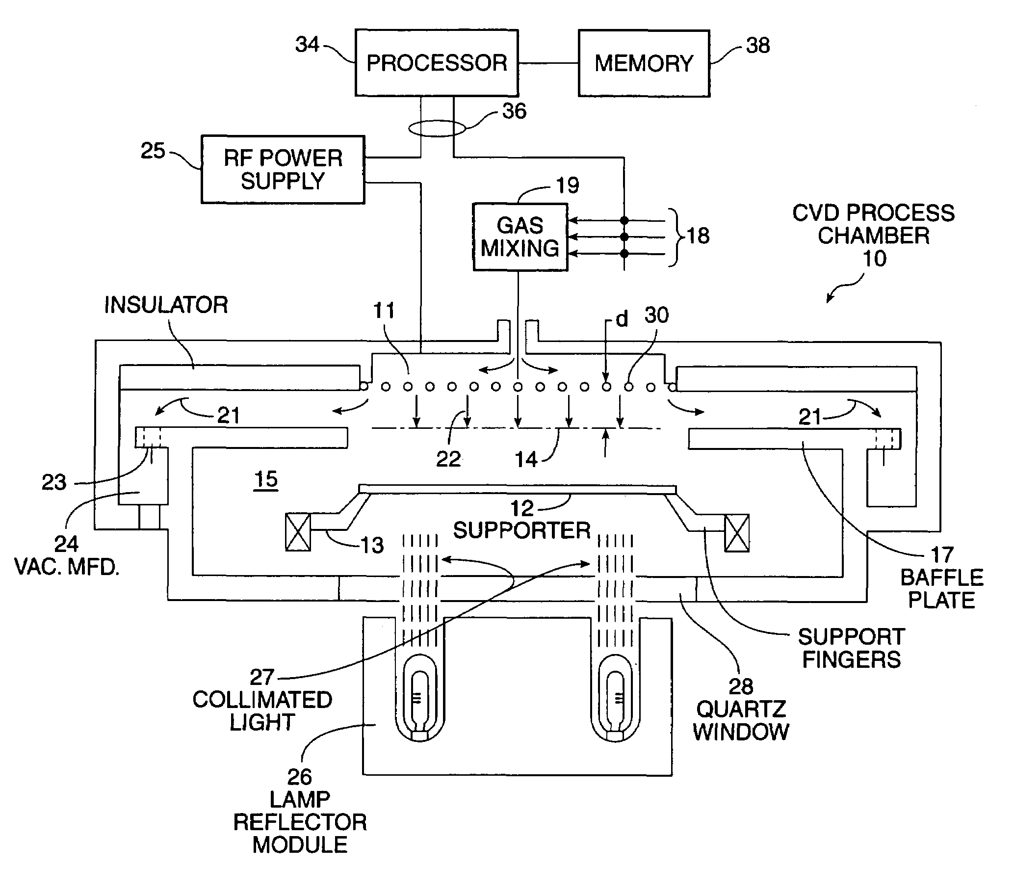
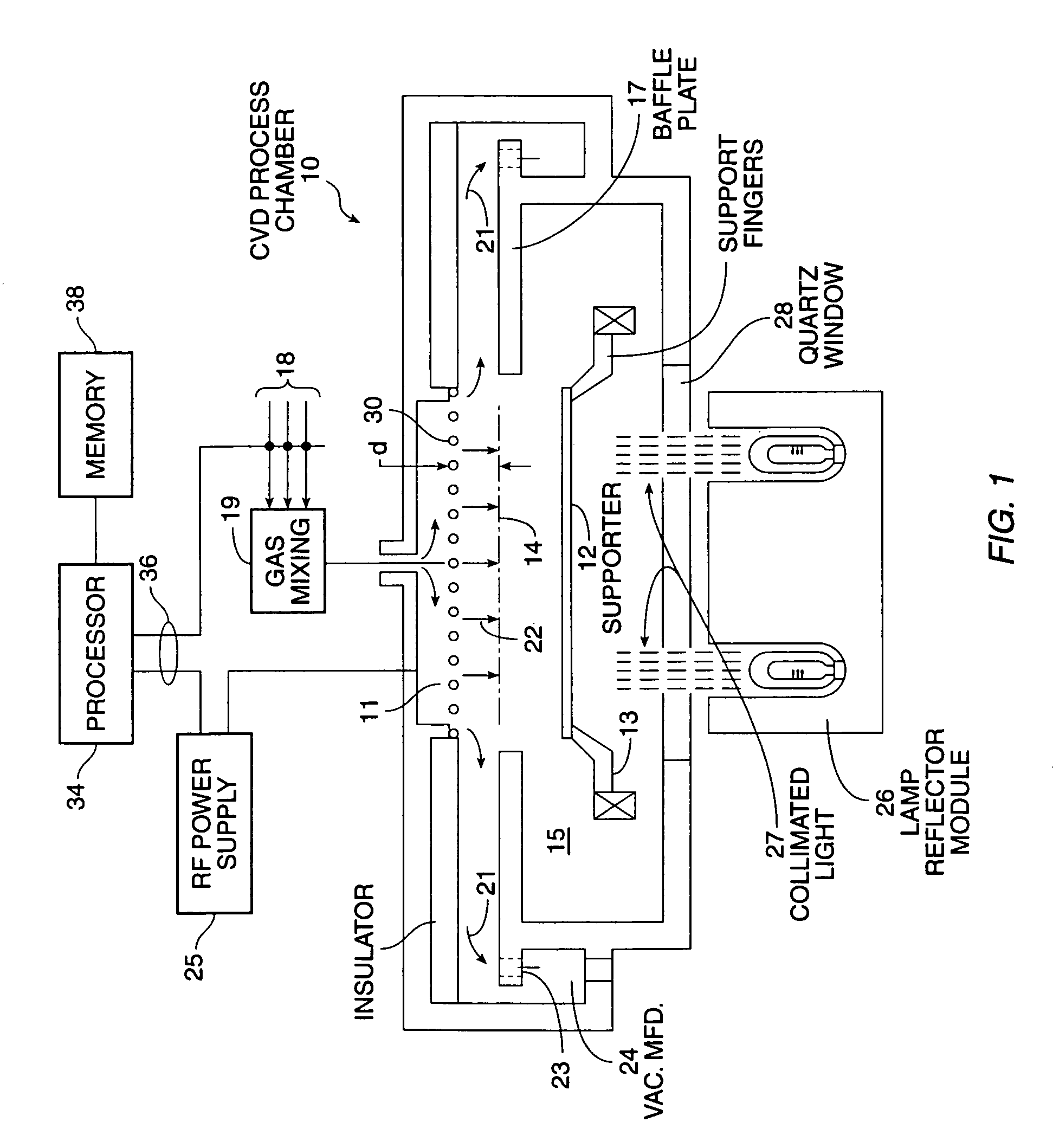
[0019]A preferred embodiment of the process for depositing an ARL according to the present invention comprises apparatus for and the use of plasma-enhanced chemical vapor deposition (PECVD) technique to bring about a chemical reaction between SiH4 and N2O, in the presence of He, with the SiH4 to N2O ratio being between about 0.5 to 3.0 and preferably 1.0. The process further includes the addition of NH3, N2, and He gases. FIG. 1 illustrates one embodiment of a simplified, parallel plate PECVD system 10 having a vacuum chamber 15 in which the antireflective layer can be deposited according to the present invention.

[0020]System 10 contains a gas distribution manifold 11 for dispersing the deposition gases to a substrate, not shown, but which is placed flat on the supporter 12. The supporter 12 is highly heat-responsive and is mounted on supports 13 so that supporter 12 (and the substrate supported on the upper surface of supporter 12) can be controllably moved between a lower loading / ...


PUM

PropertyMeasurementUnit
pressureaaaaaaaaaa
pressureaaaaaaaaaa
temperatureaaaaaaaaaa

Abstract

This invention provides a stable process for depositing an antireflective layer. Helium gas is used to lower the deposition rate of plasma-enhanced silane oxide, silane oxynitride, and silane nitride processes. Helium is also used to stabilize the process, so that different films can be deposited. The invention also provides conditions under which process parameters can be controlled to produce antireflective layers with varying optimum refractive index, absorptive index, and thickness for obtaining the desired optical behavior.

Description

CROSS REFERENCE TO RELATED APPLICATION[0001]This application is a divisional of U.S. application Ser. No. 08 / 672,888, filed Jun. 28, 1996 now U.S. Pat. No. 5,968,324, which is a continuation-in-part patent application of U.S. application Ser. No. 08 / 567,338, filed Dec. 5, 1995 now abandoned, entitled “Anti-Reflective Coating and Method for Depositing Same.”BACKGROUND OF THE INVENTION[0002]The present invention relates to apparatus for, and the processing of, semiconductor wafers. In particular, the invention relates to the deposition of antireflective layers during wafer processing.[0003]In the manufacture of integrated circuits, photolithographic techniques are used to define patterns for layers in an integrated circuit. Typically, such photolithographic techniques employ photoresist or other light-sensitive material. In conventional processing, the photoresist is first deposited on a wafer, and then a mask having transparent and opaque regions which embody the desired pattern, is ...

Claims


Application Information

Patent Timeline
Patent Type & Authority Patents(United States)
IPC IPC(8): C23C16/52C23F1/00H01L21/306C23C16/50G03F7/11G02B1/11G03F7/09H01L21/02H01L21/027
CPCG03F7/091H01L21/20
Inventor CHEUNG, DAVIDFENG, JOEHUANG, JUDY H.YAU, WAI-FAN
Owner APPLIED MATERIALS INC
Why Eureka
Try Eureka