Process for manufacturing a solar cell

a solar cell and manufacturing technology, applied in the field of manufacturing a solar cell, can solve the problems of low-cost cz wafers to be used, inability to compensate for aluminum doping, and performance impairments

Inactive Publication Date: 2006-07-04
BP ALTERNATIVE ENERGY INT
View PDF5 Cites 68 Cited by
  • Summary
  • Abstract
  • Description
  • Claims
  • Application Information

AI Technical Summary

Benefits of technology

[0022]By subjecting the cell to the Group V element doping after deposition of the aluminium layer, a number of significant advantages are achieved. The absence of the Group V element doping prior to the deposition of the aluminium layer means that the aluminium doping is not compensated by the presence of doped Group V element on the rear surface. Additionally, the requirement for a silicon oxide or silicon nitride coating on the rear surfa

Problems solved by technology

The absence of the Group V element doping prior to the deposition of the aluminium layer means that the aluminium doping is not compensated by the presence of doped Group V element on the rear surface.

Method used


Image

  • Process for manufacturing a solar cell
  • Process for manufacturing a solar cell

Examples


examples 1 – 3

EXAMPLES 1–3

[0038]147 cm2 area solar cells were prepared under varying conditions using the following general process.

Starting Material

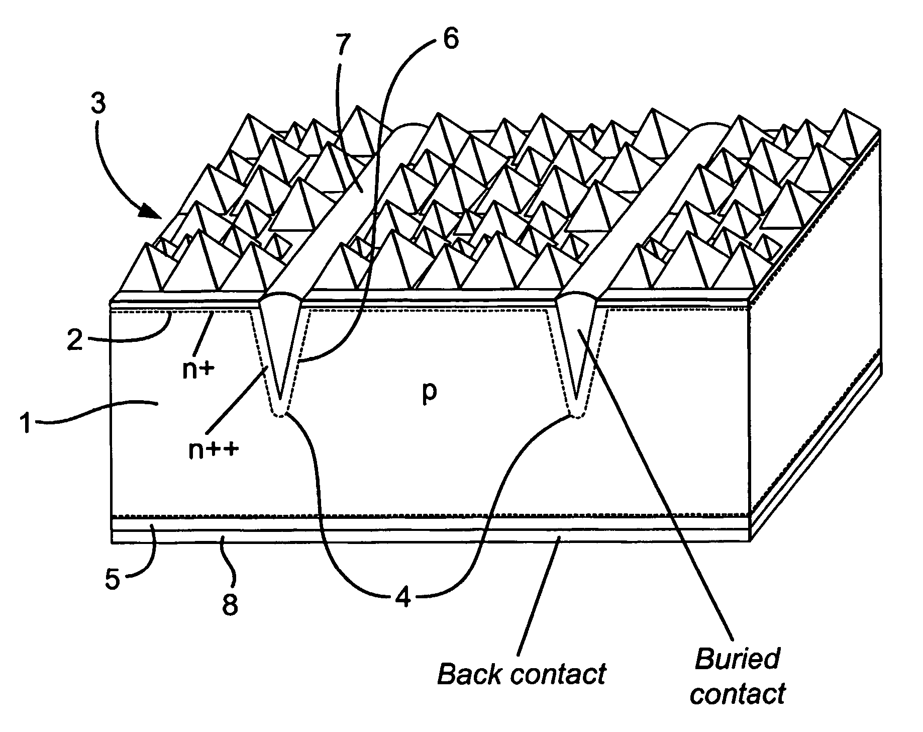
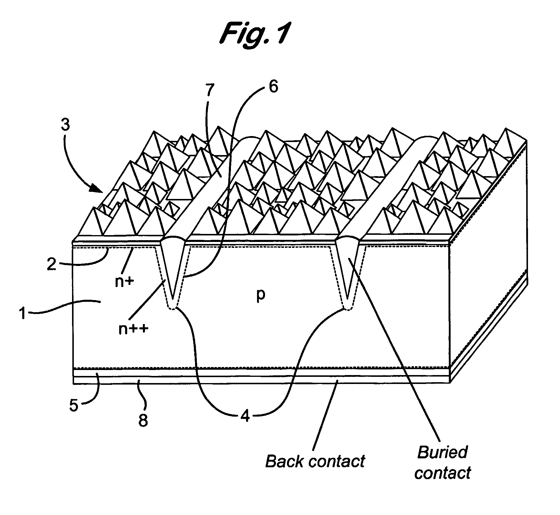
[0039]Use was made of conventional CZ silicon wafers doped p-type with boron to a resistivity of 1.2 ohm.cm and grown with [100] crystal planes parallel to the wafer surface. The wafer dimensions were 127 mm square with rounded comers of a diameter 150 mm. The wafer thickness was 300 μm. Such wafers are commercially available, for example from Bayer Solar GmbH, PV Silicon GmbH or Pillar.

Wafer Surface Preparation

[0040]The wafers were anisotropically “texture” etched in a solution of sodium hydroxide and propanol at a temperature of 90° C. and cleaned by subsequent immersions in hydrofluoric acid and hydrochloric acid with intermediate and final rinsing in deionized water followed by drying.

Phosphorus Doping and Silicon Nitride Deposition

[0041]Wafers were placed in pairs (touching) in the slots in a quartz wafer carrier and treated in an atmosphere of ...

examples 4 – 11

EXAMPLES 4–11

[0055]The process of Examples 2 and 3 was repeated using a variety of sintering tempertures and times. For comparison, a cell with a BSF applied according to the prior art process as in Example 1 above was also tested. The results are shown in Table 2. It can be seen that generally, lower sintering temperatures and shorter sintering times result in higher efficiencies.

[0056]

TABLE 2Exam-Al sinteringNo. ofVoc / pletemp and timecellsIsc / AVFF(%)Eff(%)4prior art process265.1860477.116.45995° C. for 30 min95.2660978.117.06950° C. for 50 min95.2260778.516.97950° C. for 25 min105.3761378.617.68950° C. for 10 min105.4261578.717.89900° C. for 50 min105.4061578.517.710900° C. for 25 min105.4161678.417.711900° C. for 10 min115.4161678.617.8FF = Fill Factor, a measure of power out / (Isc*Voc)

No. of cells is the number of cells tested to obtain the average values given in the Table


PUM


Abstract

Process for incorporating a back surface field into a silicon solar cell by depositing a layer of aluminium on the rear surface of the cell, sintering the aluminium at a temperature between 700 and 1000° C., exposing the cell to an atmosphere of a compound of Group V element and diffusing at a temperature of between 950 and 1000°C. so as to dope exposed p-type silicon surfaces with the Group V element. The step of exposing the cell to an atmosphere of a compound of a Group V element is carried separately from the step of sintering the aluminium layer, and subsequent to the step of depositing a layer of aluminium on the rear surface of the cell.

Description

[0001]This application is the U.S. National Phase of International Application PCT / GB02 / 02673, filed 17 Jun. 2002, which designated the U.S.[0002]The present invention relates to p-n junction solar cells, and more particularly to processes for fabricating them.BACKGROUND OF THE INVENTION[0003]Photovoltaic cells made with silicon wafers for terrestrial applications usually comprise a p-type silicon wafer. One surface of the wafer is “doped” (usually with phosphorus at temperatures of 900–1000° C.) to make it n-type and produce the basic p-n junction which is the active component of the solar cell. Metal contacts are then applied to the front and rear surfaces (the n and p surfaces) to enable the photo-generated current to be carried from the cell. In the case of the front contact the metal is typically deposited as an open grid pattern to allow light to be absorbed by the exposed silicon surface. The front grid can be deposited in embedded grooves to reduce grid shading losses. This ...

Claims


Application Information

Patent Timeline
IPC IPC(8): H01L21/00H01L31/04H01L31/068H01L31/18
CPCH01L31/068H01L31/1804Y02E10/547Y02P70/50
Inventor MASON, NIGEL BRUNELRUSSELL, RICHARD WALTER JOHN
Owner BP ALTERNATIVE ENERGY INT
Why Eureka
Try Eureka