Eureka AIR delivers breakthrough ideas for toughest innovation challenges, trusted by R&D personnel around the world.

High linearity digital variable gain amplifier

a digital variable gain and amplifier technology, applied in the direction of amplifiers with min 3 electrodes or 2 pn junctions, instruments, electric/magnetic computing, etc., can solve the problems of undesirable distortion of the amplified signal, the limited range of frequencies of prior art amplifiers, and the inability to provide linear amplification over a substantial range of circuit conditions, etc., to achieve the effect of increasing the range of input voltage signals, reducing headroom, and high linearity

Inactive Publication Date: 2006-07-04
ANALOG DEVICES INT UNLTD CO
View PDF2 Cites 8 Cited by
  • Summary
  • Abstract
  • Description
  • Claims
  • Application Information

AI Technical Summary

Benefits of technology

[0015]One object of the present invention is to provide a compact variable gain transconductance amplifier that exhibits a high level of linearity over an increased range of input voltage signals, improved (e.g., minimized) headroom, and that is capable of operating at high frequencies and varying temperatures.
[0016]One embodiment of the present invention is a composite NPN amplifier circuit that has minimal complexity (e.g., a minimal number of circuit components) and is capable of operating at a very high unity gain frequencies (e.g., frequency of a device at which ICOLLECTOR / IBASE is 1). More particularly, a composite amplifier constructed in accordance with the principles of the present invention contains many of the advantages of a single transistor and operates similar to a single transistor. However, performance enhancing components are integrated into the composite transistor amplifiers of the present invention. For example, a composite amplifier of the present invention has excellent linearity due to an enhanced transconductance.
[0017]Another embodiment of the present invention is a cascode stage composite transistor amplifier which, similar to the embodiment described above, provides excellent linearity over a larger voltage swing than conventional amplifier topologies. In the cascode stage amplifier topology, the circuit is preferably designed to provide compensation for the base current of the transistor whose collector terminal provides the output of the cascode amplifier. In this manner, a greater voltage swing at the output is possible without degradation of the signal being amplified.
[0019]Another object of the present invention is to provide amplifiers which operate substantially uniformly regardless of their placement on an integrated circuit. In preferred embodiments, the present invention biases each amplifier (e.g., the one-stage amplifier described above) with a separate bias source that provides a stabilized current regardless of temperature. In doing so, temperature does not affect the performance of multiple amplifiers constructed in accordance with the principles of the present invention and included in different locations on the same integrated circuit.

Problems solved by technology

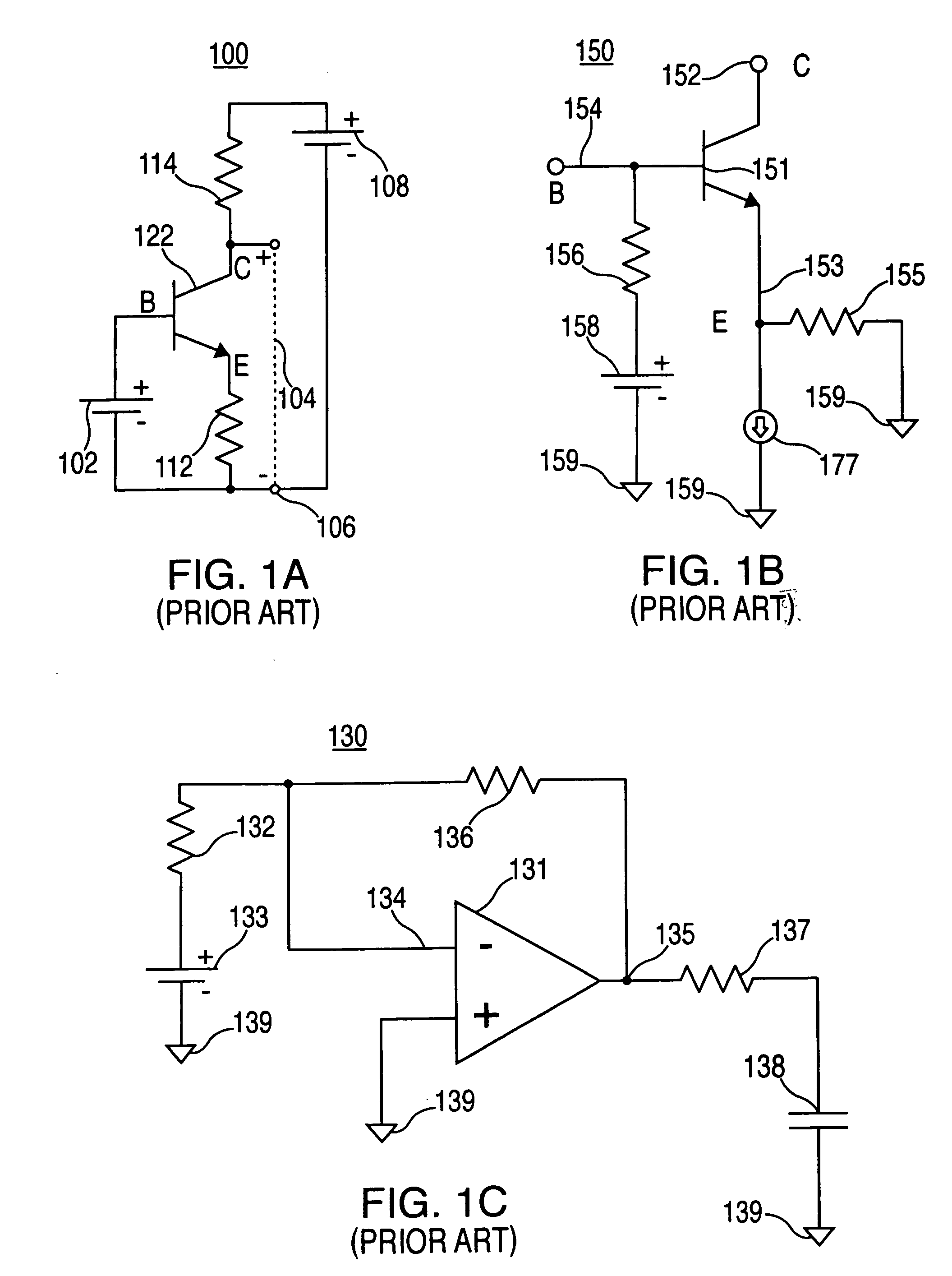
One disadvantage associated with using amplifier 100 relates to its inability to provide linear amplification over a substantial range of circuit conditions because it fails to preserve the original signal by a known gain, which is generally measured as the ratio of the output signal to the input signal of the amplifier, over the range of circuit conditions.
Single transistor prior art amplifiers do not exhibit a high level of linearity and, as a result, often introduce undesirable distortions into the amplified signal.
Thus, prior art amplifiers are greatly limited in the range of frequencies that they can successfully copy and enhance.
However, resistor 155 limits the range of signals that can be present at base terminal 154 of transistor 151, decreases gain (by increasing the voltage present at base terminal 154 of transistor 151), and contributes to noise degradation in amplifier 150.
However, in stabilizing linearity, amplifier circuit 130 does not provide a way to change its gain.

Method used


Image

  • High linearity digital variable gain amplifier
  • High linearity digital variable gain amplifier
  • High linearity digital variable gain amplifier

Examples


Embodiment Construction

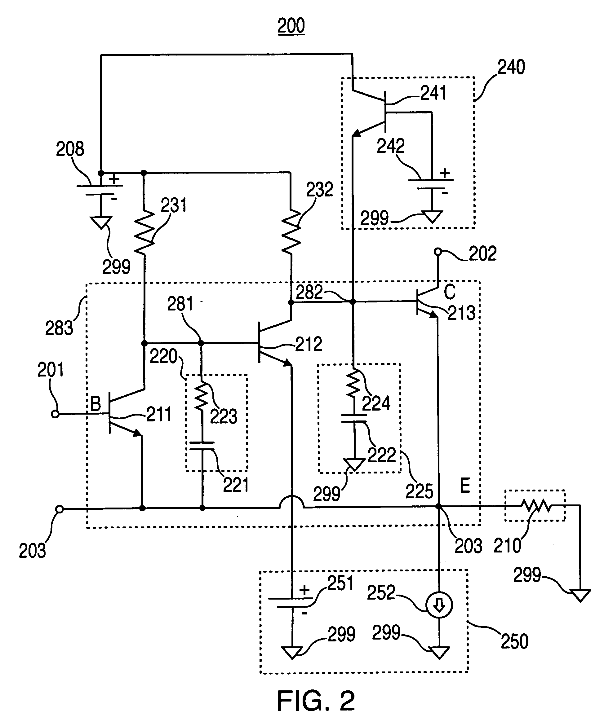
[0039]FIG. 2 depicts amplifier 200 that is constructed to include enhanced composite NPN transistor 283 that amplifies a voltage signal at input 201 to a current signal at output 202. Amplifier 200 is a compact amplifier structured around a composite NPN transistor that is capable of operating at a very high unity gain frequencies (e.g., frequencies of approximately 1 GHz to 2 GHz).

[0040]One example of applications in which amplifier 200 or composite transistor 283 may be beneficial are in applications operating at intermediate frequencies (e.g., frequencies of approximately 600 MHz to 1 GHz). As will be discussed below, amplifier 200 and composite transistor 283 may be configured in various topologies and modified to optimize, for example, gain, linearity, unity gain frequency, power, transconductance, transresistance, and noise characteristics.

[0041]Enhanced composite transistor 283 preferably includes transistor 211, which defines the base terminal of composite transistor 283 at ...


PUM


Abstract

Variable gain amplifiers offering high frequency response with improved linearity and reduced power dissipation are provided. An amplifier is disclosed that is constructed from a one-stage topology with multiple signal paths and compensation networks for improved linearity and stable operation. In this amplifier, improved performance is obtained by replacing single transistor components with enhanced active devices which incorporate local negative feedback. One embodiment of the invention is a transconductance enhancement circuit that improves transconductance and input impedance relative to the prior art. A further development is an enhanced active cascode circuit that provides improved linearity. A high frequency bipolar transistor switch is also disclosed that incorporates lateral PNP transistors as high frequency switches with improved OFF-state to ON-state impedance ratio to realize a variable gain function. These circuits are combined in an amplifier circuit that provides variable gain and high frequency performance, with improved linearity, gain, and input impedance.

Description

BACKGROUND OF THE INVENTION[0001]The present invention relates to variable gain amplifiers. More particularly, the present invention relates to amplifiers with a high linearity and efficiency over a wide range of voltage levels that can be constructed in a variety of different topologies. One such topology is a grounded input active cascode configuration that increases gain while maintaining a high level of linearity. Another such topology is a composite NPN transistor configuration that realizes minimum complexity, high unity gain, and enhanced transconductance.[0002]Amplifiers are used in a wide variety of applications. Generally, amplifiers are employed in applications where the voltage or current of a signal needs to be increased. One such application exists, for example, in communication transmitters where the voltage levels of audio signals are “weak” and need to be amplified so that they may be transmitted over relatively long distances. As per another example, a radio amplif...

Claims


Application Information

Patent Timeline
Patent Type & Authority Patents(United States)
IPC IPC(8): H03F3/04H03F1/22H03G3/10H03F1/32H03F3/343H03G1/00
CPCH03F1/22H03G1/0088H03F1/34H03F3/211H03F3/3432H03F3/4508H03F3/45103H03F3/45197H03F1/3211H03F2203/45024H03F2203/45031H03F2203/45056H03F2203/45134H03F2203/45221H03F2203/45244H03F2203/45288H03F2203/45311H03F2203/45352H03F2203/45731
Inventor SEREMETA, DORIN
Owner ANALOG DEVICES INT UNLTD CO
Why Eureka
Eureka Blog
Learn More