Light-emitting device

a technology of light-emitting devices and semiconductors, which is applied in the direction of semiconductor devices, semiconductor/solid-state device details, electrical devices, etc., can solve the problems of reducing the yield of light-emitting devices, increasing production costs, and difficult to decrease the thickness of devices, so as to achieve low cost, reduce thickness, and produce good yield

Inactive Publication Date: 2006-07-18
PANASONIC CORP
View PDF22 Cites 47 Cited by
  • Summary
  • Abstract
  • Description
  • Claims
  • Application Information

AI Technical Summary

Benefits of technology

[0010]Therefore, with the foregoing in mind, it is an object of the present invention to provide a light-emitting device with reduced thickness as a

Problems solved by technology

However, the above-mentioned configuration has the following problems.
Furthermore, with the conventional configuration, it is required that the sealant 24 is formed after wire bonding, which increases a production cost.
These problems lead to main factors for decreas

Method used


Image

  • Light-emitting device
  • Light-emitting device
  • Light-emitting device

Examples


embodiment 1

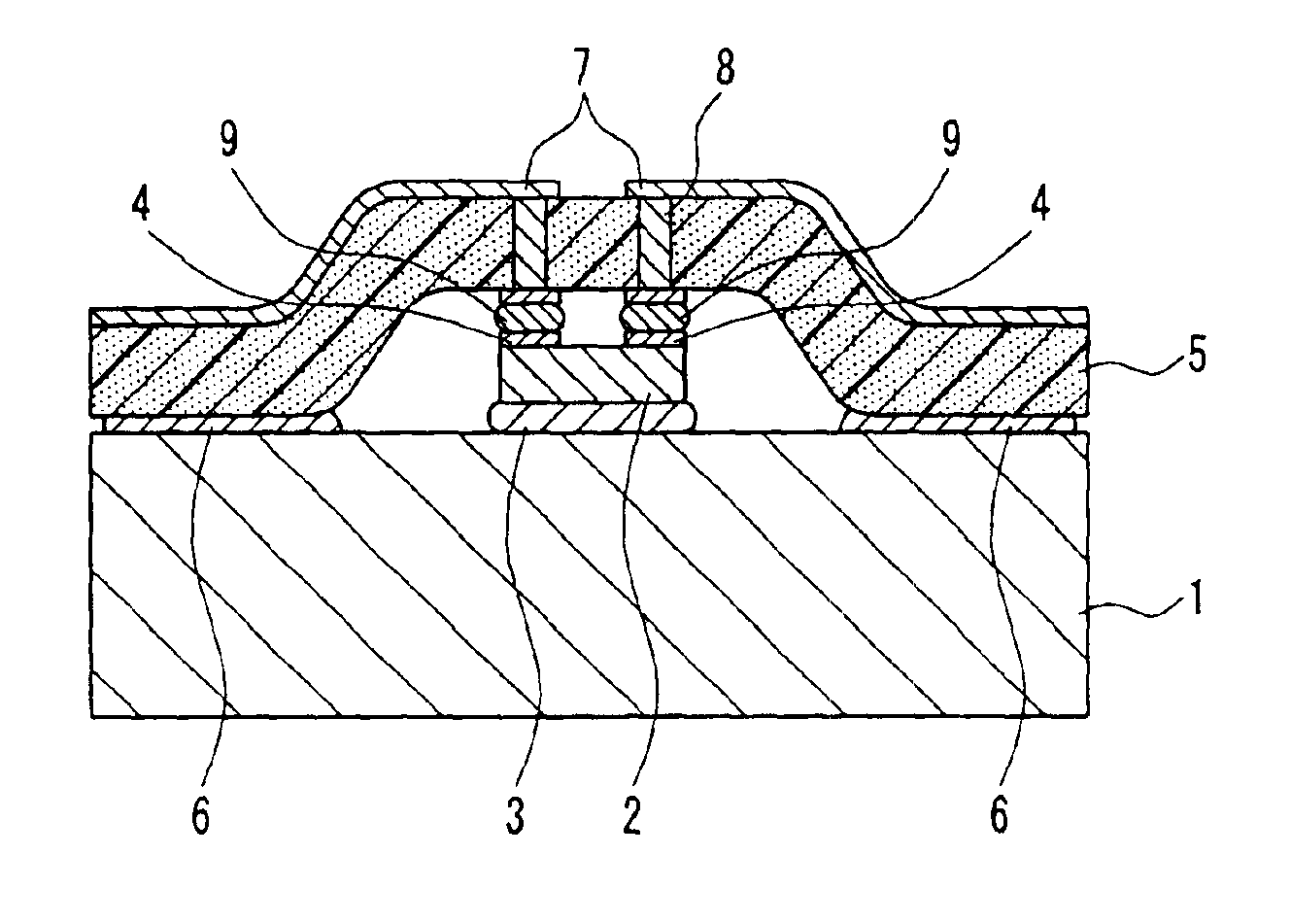
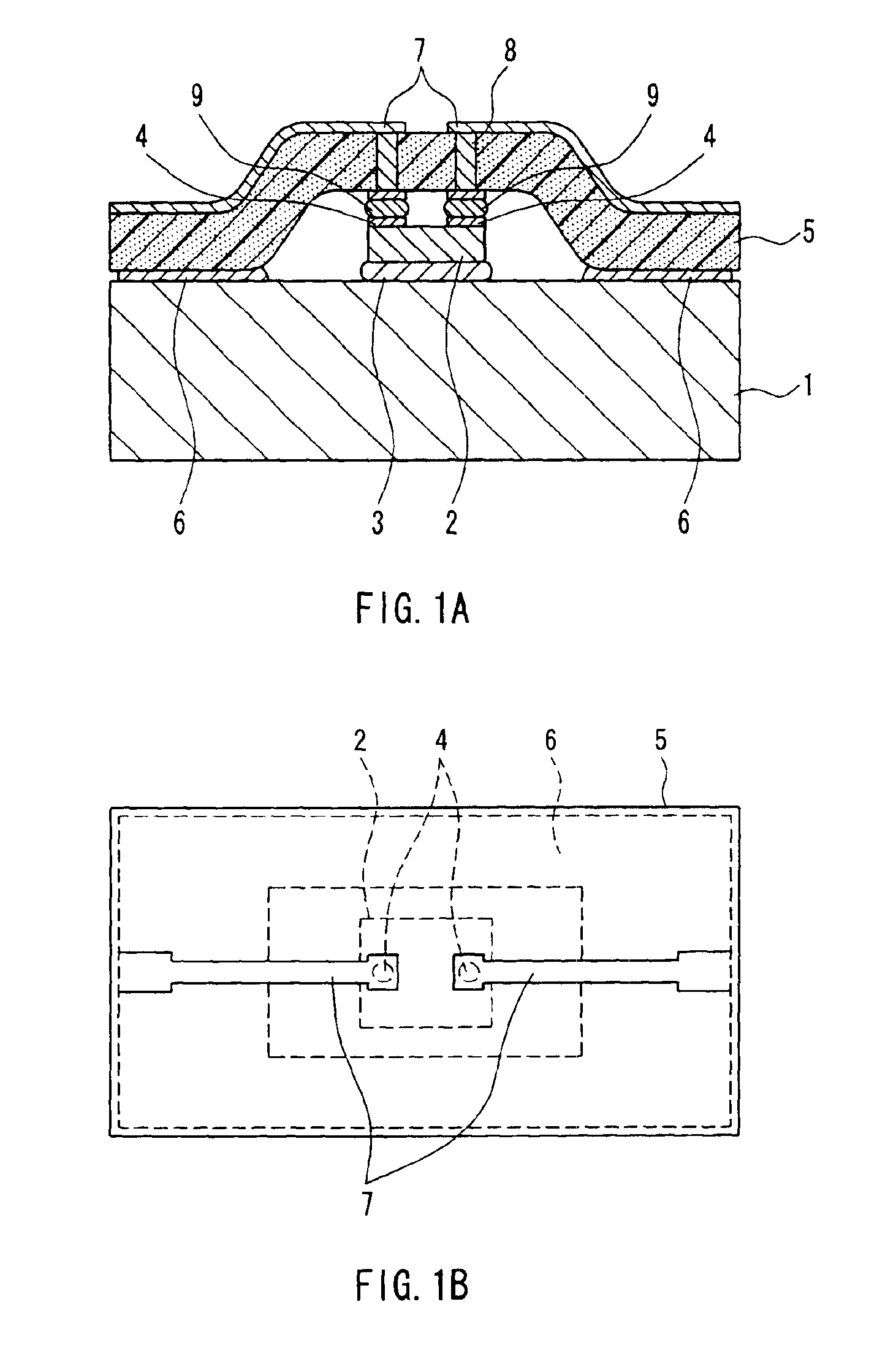
[0035]FIG. 1A is a cross-sectional view showing a light-emitting device according to Embodiment 1 of the present invention, and FIG. 1B is a plan view thereof. A semiconductor light-emitting element, such as an InGaN-based light-emitting diode 2 that emits light in blue, is fixed to a support substrate 1 with a silver paste 3. A transparent film 5 made of resin that is transparent to blue light is placed so as to cover an upper portion of the light-emitting diode 2, and fixed to the support substrate 1 with an adhesive 6. An electrode pattern 7 is formed on a surface of the transparent film 5. The electrode pattern 7 extends to a reverse surface of the transparent film 5 through through-holes 8 immediately above the light-emitting diode 2, and is electrically connected to terminal electrodes 4 of the light-emitting diode 2 through gold bumps 9. A powdery phosphor pigment is mixed in the transparent film 5 in a ratio in accordance with the level of white light to be obtained.

[0036]Ac...

embodiment 2

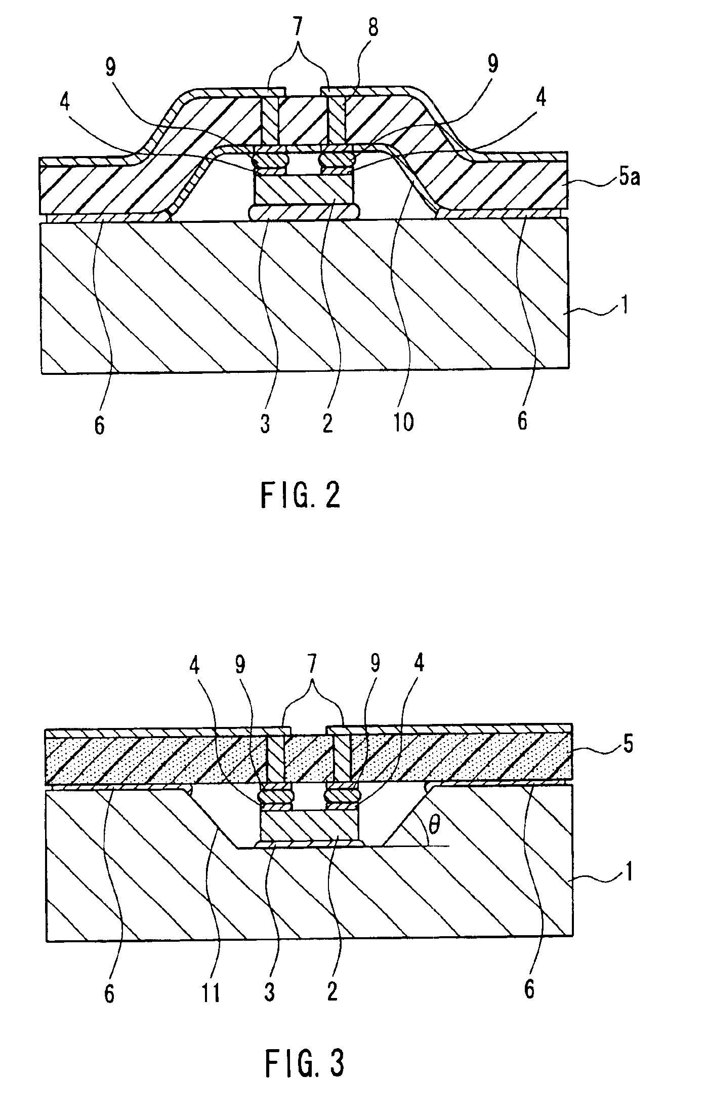
[0039]FIG. 2 is a cross-sectional view showing a light-emitting device according to Embodiment 2 of the present invention. Embodiment 2 is different from Embodiment 1 in that a transparent film 5a does not contain a phosphor pigment, and a phosphor film 10 is formed in a thin film shape on a surface of the transparent film 5a.

[0040]According to the above-mentioned configuration, the strength of the transparent film 5a can be prevented from being degraded when a large amount of phosphor is contained in the transparent film 5a. Furthermore, any amount of phosphor can be used.

[0041]The phosphor film 10 may be provided on an upper surface of the transparent film 5a. However, in the case where the phosphor film 10 is provided on a lower surface of the transparent film 5a (i.e., on a surface of the transparent film 5a on the light-emitting diode 2 side), the following advantage is obtained. Light emitted from the light-emitting diode 2 can be converted to visible light on a wavelength si...

embodiment 3

[0043]FIG. 3 is a cross-sectional view of a light-emitting device according to Embodiment 3 of the present invention. Embodiment 3 is different from Embodiment 1 in that a concave portion 11 is formed in the support substrate 1, and the light-emitting diode 2 is mounted on a bottom surface of the concave portion 11. For example, aluminum is used for the support substrate 1, and the concave portion 11 of about 1 mm on each side and a depth of about 100 μm substantially equivalent to the thickness of the light-emitting diode 2 can be formed by press forming. Strictly, the depth of the concave portion 11 is greater than the thickness of the light-emitting diode 2. However, a total thickness of the silver paste 3, the terminal electrodes 4, and the gold bumps 9 is substantially negligible.

[0044]With the above-mentioned configuration, light emitted sideways from the light-emitting diode 2 is allowed to be reflected from side walls of the concave portion 11 to be guided to the transparent...


PUM


Abstract

An InGaN-based light-emitting diode that emits light in blue, for example, is mounted on a support substrate as a semiconductor light-emitting element, and a transparent film is fixed to the support substrate so as to cover the semiconductor light-emitting element. An electrode pattern is formed on an upper surface of the transparent film, and the electrode pattern is electrically connected to terminal electrodes of the semiconductor light-emitting element through, for example, through-holes. The transparent film can contain a phosphor excited by light emitted from the semiconductor light-emitting element. It is not necessary to perform wire bonding for connecting the semiconductor light-emitting element to the electrode pattern and sealing with a sealant.

Description

BACKGROUND OF THE INVENTION[0001]1. Field of the Invention[0002]The present invention relates to a technique of mounting a semiconductor light-emitting element such as a light-emitting diode and a plane-emitting laser that can be used in, for example, a semiconductor device, an illumination device, a display device, and the like.[0003]2. Description of the Related Art[0004]In recent years, due to the advancement of semiconductor technology, a light-emitting diode and a plane-emitting diode that emit light in a blue to ultraviolet short-wavelength range have been realized. By using them, white light sources utilizing the excitation of phosphors are being developed extensively. For example, white light can be obtained by coating a blue light-emitting diode with a phosphor that emits light in yellow. Because of this, white light sources are being put into practical use for various kinds of displays and illumination. Furthermore, the following attempt also has been made: an ultraviolet ...

Claims


Application Information

Patent Timeline
IPC IPC(8): H01L33/00H01L33/50H01L33/54H01L33/62
CPCH01L24/24H01L33/505H01L33/54H01L33/62H01L2924/3025H01L2924/12041H01L2224/45144H01L2224/73265H01L2924/01322H01L2224/18H01L2224/48091H01L2924/01013H01L2924/01025H01L2924/01029H01L2924/0103H01L2924/01033H01L2924/01049H01L2924/01079H01L2924/01082H01L2924/01047H01L2924/01063H01L2924/00014H01L2924/00H01L24/20H01L2224/04105H01L2224/32245H01L2224/73267H01L2924/12042
Inventor YURI, MASAAKIUEDA, DAISUKE
Owner PANASONIC CORP
Why Eureka
Try Eureka