Power module

a power module and power technology, applied in the direction of power conversion systems, semiconductor/solid-state device details, power conversion systems, etc., can solve the problems of reducing the longevity of the power module, reducing heat transfer, and increasing the size of the heat sink b>2/b>ap or b>2/b>bp, so as to improve the cooling capacity of the heat sink, improve the reliability of the power transducer, and reduce the effect of power loss

Inactive Publication Date: 2006-07-25
MITSUBISHI ELECTRIC CORP
View PDF21 Cites 24 Cited by
  • Summary
  • Abstract
  • Description
  • Claims
  • Application Information

AI Technical Summary

Benefits of technology

[0032]In accordance with the first aspect, both the first power semiconductor device and the capacitor are directly disposed on the heat sink. The power module can thus be made lighter and smaller than conventional power modules wherein those components are provided independently. Further, the heat radiating action of the heat sink inhibits not only heat generation in the first power semiconductor device but also the temperature rise in the capacitor. This allows miniaturization of the capacitor, a reduction in inductance, and an increase in longevity.
[0053]It is therefore an object of the present invention to provide a compact, lightweight, and highly reliable power module.

Problems solved by technology

First is low temperature reliability during operation. More specifically, when the thermal expansion coefficient of the heat sink 2AP or 2BP differs from those of the diode(s) 1AP and the IGBT(s) 1BP, thermal stresses responsive to a temperature difference from the freezing point of solder will occur at the solder joints as above described. There is thus a problem of occurrence and progress of cracking at the solder joints through a heat cycle (or temperature cycle) in the use (or operation) of the power module 101P, 102P, 103P and / or a heat cycle by repetitions of start and halt of the power module. Such cracking at the solder joints reduces the longevity of the power module.
This brings up another problem that the size of the heat sink 2AP or 2BP must be increased.
Thus, there is a problem of reduced heat transfer because the heat-conducting grease cannot completely fill in the space between the radiating fin 2AP, 2BP and the insulating substrate(s) 5P or the base plate 9P (due to the incoming air).
Another problem is that the occurrence or progress of cracking at the solder joints, described above, may be encouraged.
The formation of clearance thus results in deterioration in the reliability of the power module.
This brings up, as has been described, another problem that the size of the heat sink 2AP, 2BP must be increased.
This causes variations in the inductance of the wiring or wires 7P from one power semiconductor device to another, thereby causing variations in output voltage.

Method used


Image

  • Power module
  • Power module
  • Power module

Examples


first preferred embodiment

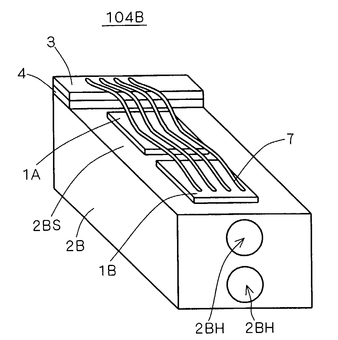
[0085]FIG. 1 is a schematic external view of a power module 101 according to a first preferred embodiment. As shown in FIG. 1, the power module 101 comprises a power semiconductor device (e.g., free-wheeling diode or IGBT) 1 formed for example of a silicon (Si) substrate, a heat sink 2A, electrodes 3, insulating layers 4, and wires 7. For the sake of simplicity, the details of the power semiconductor device 1 is not illustrated in FIG. 1.

[0086]Specifically, the power semiconductor device 1 is disposed in immediate or direct contact with the heat sink 2A. The power semiconductor device 1 has main surfaces 1S1 and 1S2 corresponding to the main surfaces of the above-mentioned silicon substrate, in each of which an electrode is formed (not shown). One main surface (hereinafter referred to as “rear surface”) 1S2 or the electrode (hereinafter referred to as “rear electrode”) formed in the rear surface 1S2 is for example soldered onto a plane surface 2AS of the heat sink 2A.

[0087]Here “dis...

second preferred embodiment

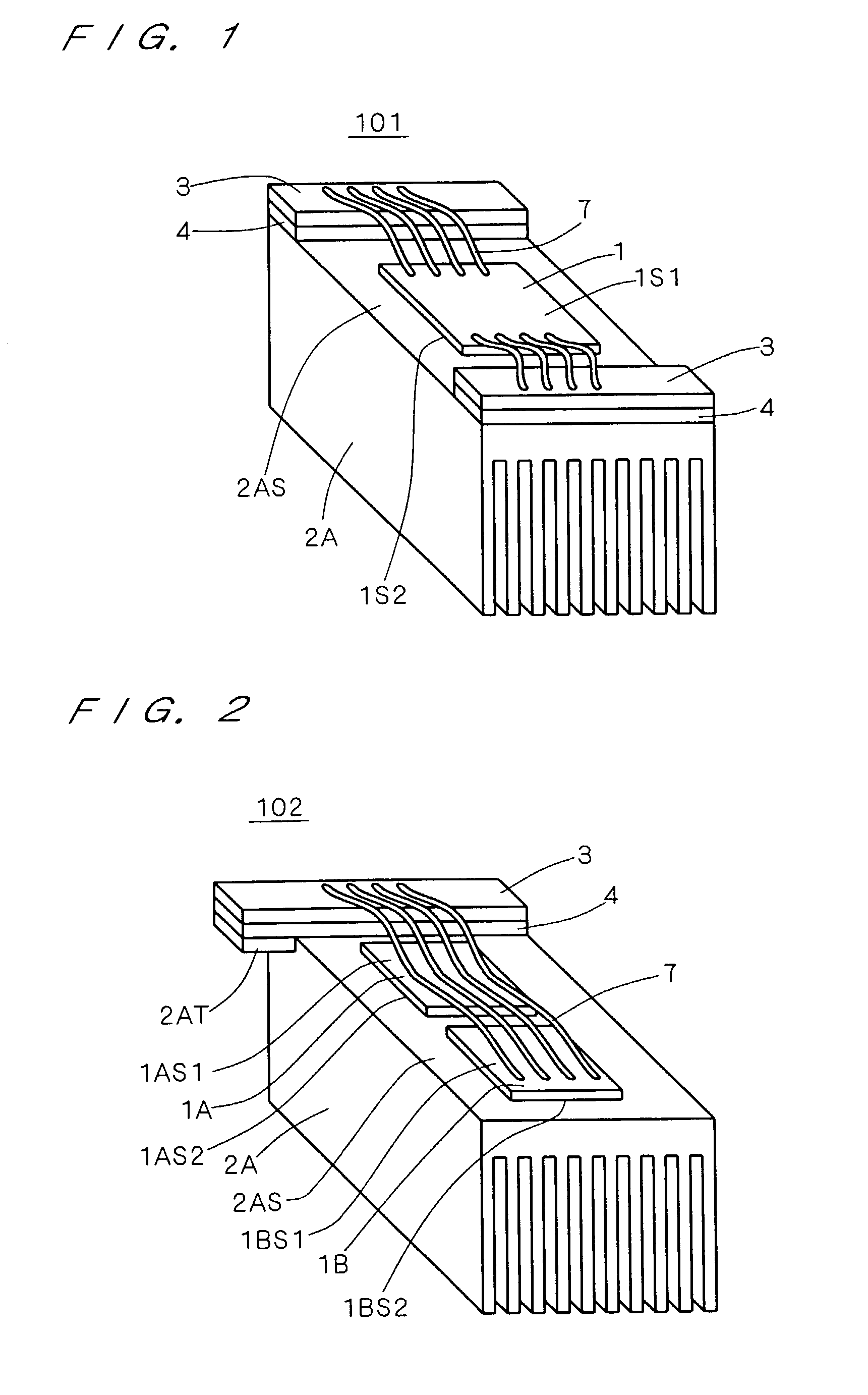
[0092]FIG. 2 is a schematic external view of a power module 102 according to a second preferred embodiment. As shown in FIG. 2, the power module 102 comprises a free-wheeling diode 1A and an IGBT 1B, serving in a pair as the aforementioned power semiconductor device 1; the heat sink 2A; the electrode 3; the insulating layer 4; and the wires 7. Components similar to those previously described are denoted by the same reference numerals and they are considered to be supported by the foregoing description.

[0093]The free-wheeling diode 1A has a front surface 1AS1 and a rear surface 1AS2 corresponding to the aforementioned front and rear surfaces 1S1 and 1S2, respectively and also has a front electrode and a rear electrode (not shown). Similarly, the IGBT 1B has a front surface 1BS1 and a rear surface 1BS2 corresponding to the aforementioned front and rear surfaces 1S1 and 1S2, respectively and also has a front electrode and a rear electrode (not shown)

[0094]Specifically, the heat sink 2A...

third preferred embodiment

[0098]FIG. 3 is a schematic external view of a power module 103 according to a third preferred embodiment. The power module 103 has such a configuration that the two power modules 102 are coupled together through an insulating member 10. The insulating member 10 may be an epoxy resin, injection molded plastic, or the like.

[0099]In the power module 103, the electrode 3 of each power module 102 extends to the other power module 102 and is electrically connected to (e.g., soldered to) the heat sink 2A of the other power module 102 (cf. protrusions 3T).

[0100]The power module 103 can easily be produced since its circuit configuration is such that the two prepared power modules 102 are merely combined together. The use of the compact and lightweight power modules 102 allows a reduction in the size and weight of the power module 103. Alternatively, three or more power modules 102 may be combined.

[0101]The diodes 1A and the heat sinks 2A may directly be connected with each other by the wire...


PUM


Abstract

In a power module (111), a free-wheeling diode (1A), an IGBT (1B), and a capacitor (20) for smoothing direct current are disposed directly on a surface (2BS) of a conductive heat sink (2B) with through holes (2BH). The rear electrodes of the free wheeling diode (1A), the IGBT (1B), and the capacitor (20) are bonded to the heat sink (2B) for example with solder, whereby the diode (1A), the IGBT (1B), and the capacitor (20) are electrically connected with the heat sink (2B). The front electrodes of the diode (1A), the IGBT (1B), and the capacitor (20) are connected with each other for example by wires (7). In the heat sink (2B), a cooling medium flows through the through holes (2BH). Such a configuration allows miniaturization of the power module and improves the cooling performance and reliability of the power module.

Description

BACKGROUND OF THE INVENTION[0001]1. Field of the Invention[0002]The present invention relates to power modules and especially to techniques for improving cooling performance of power modules.[0003]2. Description of the Background Art[0004]FIG. 34 is a schematic external view of a first conventional power module 101P. In the power module 101P, a copper base plate 9P is disposed through a heat-conducting grease (not shown) over a radiating fin or heat sink 2AP, and an insulating substrate 5P is disposed on the base plate 9P. On the insulating substrate 5P, there are disposed a freewheeling diode 1AP (hereinafter also referred to as “diode”) and an insulated gate bipolar transistor 1BP (hereinafter referred to as “IGBT”).[0005]In the conventional power module 101P, copper foils 6P are placed on both main surfaces of the insulating substrate 5P. The base plate 9P and the copper foil 6P are bonded together with solder, and the diode 1AP and the IGBT 1BT are soldered onto the copper foil ...

Claims


Application Information

Patent Timeline
Patent Type & Authority Patents(United States)
IPC IPC(8): H01L23/34H01L23/36H01L23/473H01L25/00H01L25/07H02M1/00H02M7/48
CPCH01L23/473H01L25/072H01L24/49H01L24/48H01L2223/6622H01L2224/48091H01L2224/48137H01L2224/48227H01L2224/4824H01L2224/49111H01L2224/49175H01L2924/01004H01L2924/01005H01L2924/01006H01L2924/01013H01L2924/01014H01L2924/01016H01L2924/0102H01L2924/01029H01L2924/01042H01L2924/01047H01L2924/01074H01L2924/13055H01L2924/19041H01L2924/19043H01L2924/19105H01L2924/30107H01L2224/48472H01L2924/01033H01L2924/01068H01L2924/014H01L2924/1305H01L2924/00014H01L2924/00H01L2924/00012H01L2224/48139H01L2924/351H01L2924/181H05K7/14329H01L2224/45099H01L2224/05599
Inventor FUKADA, MASAKAZUNAKAJIMA, DAITAKANASHI, KEN
Owner MITSUBISHI ELECTRIC CORP
Why Eureka
Try Eureka