Method and apparatus for controlling electron beam current

a technology of electron beam current and control method, which is applied in the direction of static indicating device, tomography, instruments, etc., can solve the problems of limiting the resolution of modern x-ray imaging, difficult focusing to a small spot size, and inefficient process of x-ray generation, etc., and achieves the effect of high electron beam current density and high electron current density

Inactive Publication Date: 2006-08-01
THE UNIV OF NORTH CAROLINA AT CHAPEL HILL
View PDF37 Cites 109 Cited by
  • Summary
  • Abstract
  • Description
  • Claims
  • Application Information

AI Technical Summary

Benefits of technology

[0028]The present invention avoids the undesirable features of current x-ray generating devices by incorporating a field emission nanostructure cathode material into an x-ray generating device. The nanostructure field emission material of the present invention is capable of producing, in a controlled and reliable manner, a high emitted electron current density through the application of a relatively small control electrical field. Therefore, a substantially higher electron beam current can be achieved compared with that of t

Problems solved by technology

However, the thermionic origin of the electrons makes focusing to a small spot size difficult.
This, in part, limits the resolution of modern x-ray imaging (see, for example, Radiologic Science For Technologist, S. C. Bushong, Mosby-Year Book, 1997).
This process of x-ray generation is not very efficient since about 98 percent of the kinetic energy of the electron stream is converted upon impact with the anode into thermal energy.
As noted above, a shutter (e.g. 275) is necessary in such devices because thermionic emission of electrons from a cathode does not allow for precise step function initiation and termination of the resulting electron beam.
Indeed, while still at elevated temperatures and subsequent to removal of power, a thermionic cathode may emit electrons which may cause unwanted x-ray emission from the target.
Moreover, due to high temperature heating, the cathode filament has a limited lifetime, typically around a few hundred hours in medical applications and thousand hours in analytical applications.
Under normal usage, the principle factor determining the lifetime of the x-ray tube is often damage to the cathode filament.
Therefore, a principle limitation in these applications is the amount of electron beam current generated by the cathode.
However, the incorporation of conventional field emission cathode materials into x-ray generating devices presents certain challenges.
Many conventional field emission materials are incapable of producing the desired emitted electron circuit density absent the application of a relatively high electrical field to the cathode.
Moreover, many of the conventional field emission materials cannot produce stable emissions at high current densities under high applied electrical fields.
The use of high control volt

Method used


Image

  • Method and apparatus for controlling electron beam current
  • Method and apparatus for controlling electron beam current
  • Method and apparatus for controlling electron beam current

Examples


embodiment 600

[0089]In another embodiment 600, the field emission cathode structure 610 comprises a thin nanostructure or carbon nanotube paper 350 placed on a conducting substrate 300 which, preferably, has a desired metal interlayer 310 such as Fe or Ti. The paper 350 is pressed onto the substrate 300 with the metal interlayer 310, and is preferably vacuum-annealed to achieve adhesion. The paper 350 is further fixed on the substrate 300 by an insulating collar 630. A gate electrode 620, preferably a high melting temperature metal grid, is placed on the insulating collar 630. A power source 640, preferably with variable voltage control, is connected between the gate electrode 620 and paper 350 or the conducting substrate 300.

embodiment 700

[0090]Alternatively, an embodiment 700 may comprise a field emission cathode structure 710 comprising a nanostructure or carbon nanotube film 330 on a conducting substrate 300, preferably with a desired metal interlayer 310, wherein the film 330 is patterned and aligned with the openings in a gate electrode 720 to minimize overheating of the metal grid caused by bombardment with the field emitted electrons. The gate electrode 720, preferably a high melting temperature metal grid, is placed on an insulating spacer 730. The metal grid 720 and the patterned film 330 are placed in an off-set geometry to avoid the problems of overheating the grid 720 due to field emitted electrons striking the grid 720 for extended periods of time.

[0091]In yet another embodiment 800, the field emission cathode structure 810 comprises a nanostructure or carbon nanotube film 330 on a conducting substrate 300, preferably with a desired metal interlayer 310. After deposition, the film 330 is preferably vacuu...

first embodiment

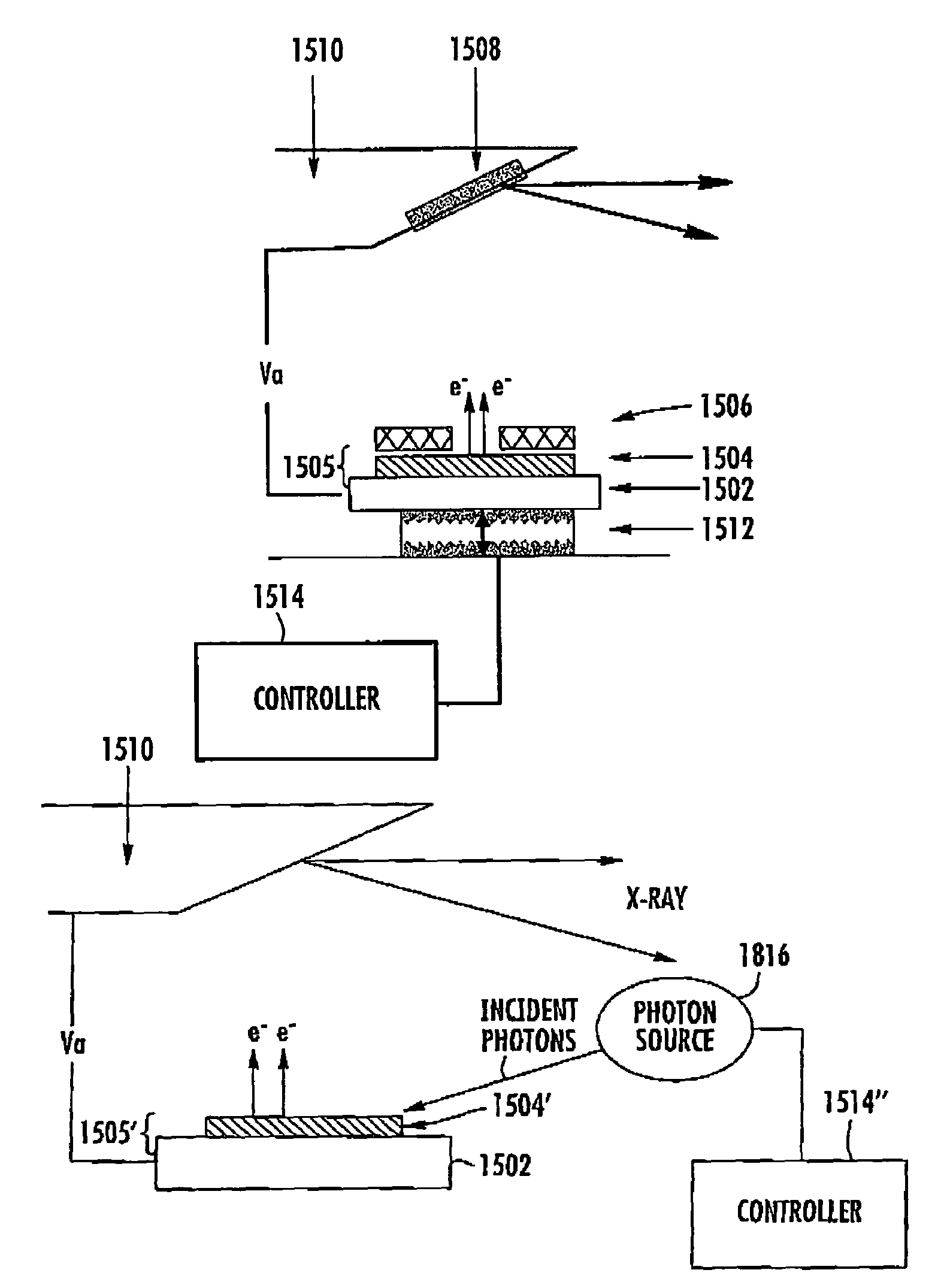
[0122]In accordance with the present invention, a voltage Va is established between cathode 1505 and anode 1508. For a given voltage V and a distance D between the anode and the cathode, the applied electric field, i.e., the x-ray energy, is E=V / D. In electron field emission the electron emission current I is related to the applied electric field E through the Fowler-Nordheim equation as follows:

J=aE2exp(−bφ3 / 2 / E)

where J is the emitted electron current, φ is the work function of the field emission materials, E is the applied electric field, and a and b are Fowler-Nordheim parameters which are dependent upon the particular setup geometry and nanostructures of the emissive materials. One of ordinary skill in the art knowing the particular setup geometry and the nanostructure of the emissive materials can readily determine a and b.

[0123]Accordingly, it can be seen that the electric field E is proportional to the voltage applied between the cathode and anode (Va), and inversely proporti...


PUM


Abstract

An x-ray generating device includes a field emission cathode formed at least partially from a nanostructure-containing material having an emitted electron current density of at least 4 A/cm2. High energy conversion efficiency and compact design are achieved due to easy focusing of cold cathode emitted electrons and dramatic reduction of heating at the anode. In addition, by pulsing the field between the cathode and the gate or anode and focusing the electron beams at different anode materials, pulsed x-ray radiation with varying energy can be generated from a single device. Methods and apparatus for independent control of electron emission current and x-ray energy in x-ray tubes are also provided. The independent control can be accomplished by adjusting the distance between the cathode and anode. The independent control can also be accomplished by adjusting the temperature of the cathode. The independent control can also be accomplished by optical excitation of the cathode. The cathode can include field emissive materials such as carbon nanotubes.

Description

[0001]This application is a continuation-in-part of U.S. application Ser. No. 09 / 679,303, entitled “X-Ray Generating Mechanism Using Electron Field Emission Cathode,” filed on Oct. 6, 2000 now U.S. Pat. No. 6,553,096, the entire contents of which are herein expressly incorporated by reference.STATEMENT REGARDING FEDERALLY SPONSORED RESEARCH OR DEVELOPMENT[0002]At least some aspects of this invention were made with Government support under the sponsorship of the Office of Naval Research, contract no. N00014-98-1-0597. The Government may have certain rights in this invention.BACKGROUND OF THE INVENTION[0003]In the description that follows, reference is made to certain structures and / or methods. However, the following references should not be construed as an admission that these structures and / or methods constitute prior art. Applicants expressly reserve the right to demonstrate that such structures and / or methods do not qualify as prior art against the present invention.[0004]X-rays o...

Claims


Application Information

Patent Timeline
IPC IPC(8): H01J35/32G21K5/02A61B6/00A61B6/03G21K5/08H01J35/06H01J35/08H01J35/10H05G1/00H05G1/34
CPCA61B6/4021A61B6/4488A61B6/482B82Y10/00H01J3/021H01J35/06H01J35/065H01J35/08H01J35/105H01J35/14H01J35/22H01J35/28H01J35/30H05G1/34A61B6/032A61B6/405H01J2201/30469H01J2235/06H01J2235/062H01J2235/064H01J2235/068A61B6/4028H01J35/147
Inventor LU, JIANPINGZHOU, OTTOCHENG, YUAN
Owner THE UNIV OF NORTH CAROLINA AT CHAPEL HILL
Why Eureka
Try Eureka