Circuits and methods for matching device characteristics for analog and mixed-signal designs

a technology of analog and mixed signals, applied in the field of circuit layout patterns and layout, can solve the problems of non-uniform doping profiles, different threshold voltages, fluctuations in number and position of dopant atoms or random randomness of line edge roughness of devices, so as to improve the performance of analog and mixed signal circuits, eliminate or significantly minimize the sensitivity of such circuit components, and match circuit components precisely or proportionally

Inactive Publication Date: 2006-08-01
INT BUSINESS MASCH CORP
View PDF7 Cites 8 Cited by
  • Summary
  • Abstract
  • Description
  • Claims
  • Application Information

AI Technical Summary

Benefits of technology

[0006]Exemplary embodiments of the invention include circuit designs and methods that provide matching of device characteristics for, e.g., analog or mixed-signal semiconductor integrated circuit designs. In particular, exemplary embodiments of the invention include circuit layout patterns and layout methods that provide precise or proportional matching of circuit components by uniformly distributing circuit components in a manner that eliminates or significantly minimizes the sensitivity of such circuit components to environmental effects and process variations, thereby improving the performance of analog and mixed-signal circuits.
[0008]In another exemplary embodiment of the invention, the process of uniformly distributing the unit cells is performed by optimally arranging the unit cells of the components in an array structure to maximize layout symmetry of the components and render the circuit (e.g., analog circuit) insensitive to environmental effects, such as uneven lithographic patterning, ion implanting, oxidation, thermal annealing, chemical-mechanical polishing and well proximity effect.
[0009]In another exemplary embodiment of the invention, one or more circuit components can be selected as a master (reference) component whose electrical parameters are precisely transferred (1:1 ratio) or proportionally transferred (any ratio, a:b) to one or more slave components. For example, one or more slave components that have a different area ratio with respect to each other and / or the master component(s) can be uniformly distributed by dividing the components into either full-unit cells or dividing the components into sub-unit cells that are filled with dummy elements, and evenly distributing the full-unit and sub-unit cells in an array structure. For slave components that are proportionally smaller than a master component, sub-unit cells with dummy elements can be used to facilitate even distribution of such slave components in the array and around the master component.
[0010]Furthermore, in one exemplary embodiment of the invention, a master (reference) component can be placed in a central location of an array among the plurality of slave devices, so that the electrical parameters of the master component can be evenly mapped to the slave components. Furthermore, a plurality of dummy cells can be placed in empty lots in the array and around an outer perimeter of the array to minimize the well-proximity edge effect.

Problems solved by technology

For example, variations in Vt between neighboring transistors can result from fluctuations in number and position of dopant atoms or randomness in line edge roughness of devices.
Further, layout asymmetry, pattern density difference variations, and oxidation rate difference due to stress from isolation, all contribute to device mismatch to a certain degree.
These mismatches result in different threshold voltages, different current flows, different carrier mobility, and different trigger points.
Another source of mismatch is the known “well proximity effect” due to dopants being scattered along the n-well or p-well sidewalls and corners resulting in a non-uniform doping profile.
Indeed, process mismatch due to lithographic patterning, ion implantation, chemical-mechanical polishing, oxidation, or CVD deposition, makes smaller devices with short channel lengths especially prone to device mismatch problem.
On the other hand, although larger devices are not as sensitive to threshold mismatch, their capacitive loading makes them unsuitable for high-frequency operations.
Furthermore, larger devices consume more chip area and more power, which increases the cost.

Method used


Image

  • Circuits and methods for matching device characteristics for analog and mixed-signal designs
  • Circuits and methods for matching device characteristics for analog and mixed-signal designs
  • Circuits and methods for matching device characteristics for analog and mixed-signal designs

Examples


Embodiment Construction

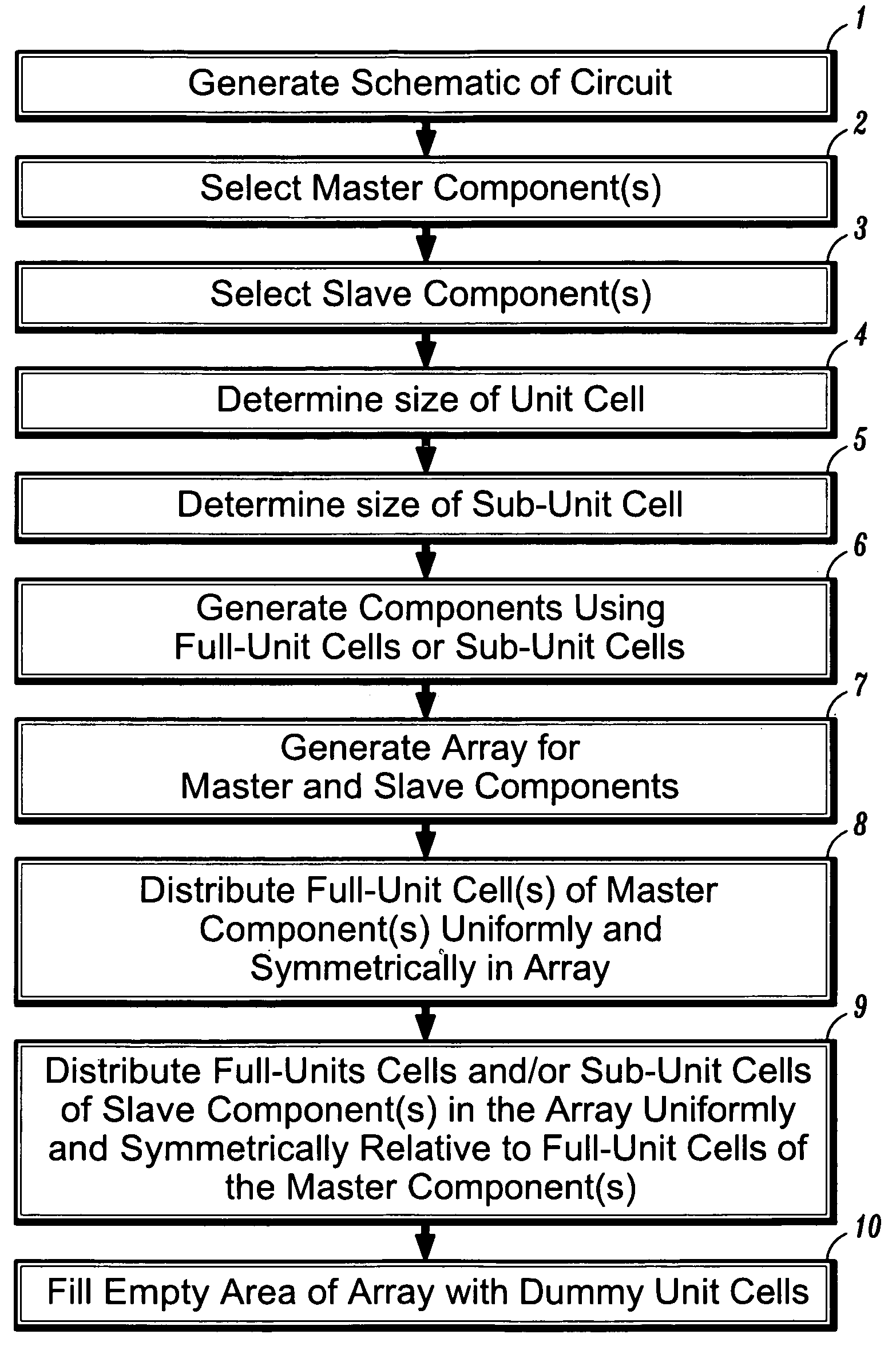
[0022]Exemplary embodiments of the invention generally include circuit designs and methods that provide matching of device characteristics for analog or mixed-signal semiconductor integrated circuits. Exemplary embodiments of the invention include circuit layout patterns and layout methods that provide precise or proportional matching of circuit components by uniformly distributing the circuit components in a manner that eliminates or significantly minimizes the sensitivity of such components to environmental effects and process variations, thereby improving the performance of analog and mixed-signal circuits.

[0023]FIG. 1 is a flow diagram illustrating a method for matching electrical characteristics of two or more components of a semiconductor integrated circuit, according to an exemplary embodiment of the invention. It is to be understood that the methods described herein with reference to FIG. 1, for example, can represent physical process steps that occur during the design and f...


PUM


Abstract

Circuit designs and methods are provided for matching device characteristics for, e.g., analog or mixed-signal semiconductor integrated circuit designs. In particular, circuit layout patterns and layout methods are provided which enable precise or proportional matching of circuit components by uniformly distributing circuit components in a manner that eliminates or significantly minimizes the sensitivity of such circuit components to environmental effects and process variations, thereby improving the performance of analog and mixed-signal circuits.

Description

TECHNICAL FIELD OF THE INVENTION[0001]The present invention relates generally to circuit designs and methods that provide matching of device characteristics for analog or mixed-signal semiconductor integrated circuits. More specifically, the invention relates to circuit layout patterns and layout methods that provide precise or proportional matching of circuit components by uniformly distributing the circuit components in a manner that eliminates or significantly minimizes the sensitivity of such components to environmental effects and process variations, thereby improving the performance of analog and mixed-signal circuits.BACKGROUND[0002]In the design of semiconductor integrated circuits, it is very important to consider variations in device characteristics (device mismatch) such as Vt (threshold voltage) for a given circuit design, in order to achieve circuit robustness and obtain high manufacturing functional yields for such devices. The matching of device characteristics is par...

Claims


Application Information

Patent Timeline
Patent Type & Authority Patents(United States)
IPC IPC(8): G06F17/50H01L21/822G06F9/45H01L21/82H01L27/04H01L27/118
CPCG06F17/5068G06F30/39
Inventor CHEN, HOWARD HAOHSU, LOUIS LU-CHENHWANG, CHARLIE CHORNGLII
Owner INT BUSINESS MASCH CORP
Why Eureka
Try Eureka