Semiconductor light emitting device, image display unit, lighting apparatus, and method of fabricating semiconductor light emitting device

a technology of semiconductor light emitting device and semiconductor light, which is applied in the direction of semiconductor/solid-state device manufacturing, semiconductor devices, electrical devices, etc., can solve the problems of inability to allow light to emerge outwardly from the device due to total reflection, failure to increase the light emergence efficiency, and difficulty in displaying images with high resolution. , to achieve the effect of improving light emergence efficiency, good crystallinity, and large quantity of light emission

Inactive Publication Date: 2006-08-08
SONY CORP
View PDF8 Cites 33 Cited by
  • Summary
  • Abstract
  • Description
  • Claims
  • Application Information

AI Technical Summary

Benefits of technology

[0015]As one example of the semiconductor light emitting device of the present invention, a crystal growth layer can be formed using a nitride semiconductor having a wurtzite type crystal structure. In particular, a tilted crystal growth layer formed by selective growth from an opening portion formed in a mask or from an under growth layer disposed on a substrate in such a manner as to be tilted from the principal plane of the substrate has good crystallinity, thereby allowing a large quantity of light emission. In the case of forming the irregularities on the back plane of the tilted crystal growth layer, the light emergence efficiency can be further increased. As a result, a light emitting device including such a tilted crystal growth layer can sufficiently achieve the performance.
[0016]The fabrication method of the present invention can be effectively applied not only to the semiconductor light emitting device having the above-described shape but also to a semiconductor light emitting device having a structure failing to increase the light emergence efficiency due to total reflection caused by a flat plane of a crystal layer. The present invention can further provide an image display unit and a lighting apparatus, wherein the above-described semiconductor light emitting devices are arrayed, each of which emits light in response to a signal.

Problems solved by technology

In particular, the latter technique has a difficulty in that if light generated in a light emission region of a semiconductor light emitting device enters a light emergence plane at a large incident angle, such light is not allowed to emerge outwardly from the device due to total reflection.
In this case, if the back plane of a crystal layer, at which the substrate is joined to the device, is taken as a light emergence plane, part of light generated in the device is not allowed to emerge outwardly from the device due to total reflection, thereby failing to increase the light emergence efficiency.
In the case of fabricating a planar image display unit requiring a light control board for adjusting the optical path in one direction or the like, in addition to each device main body including a light emission region, it is difficult to display an image with a high resolution by arraying fine devices and controlling light emission for each of the devices.
As a result, it fails to further increase the light emergence efficiency and to sufficiently achieve the performance of the device.

Method used


Image

  • Semiconductor light emitting device, image display unit, lighting apparatus, and method of fabricating semiconductor light emitting device
  • Semiconductor light emitting device, image display unit, lighting apparatus, and method of fabricating semiconductor light emitting device
  • Semiconductor light emitting device, image display unit, lighting apparatus, and method of fabricating semiconductor light emitting device

Examples


first embodiment

[First Embodiment]

[0055]A first embodiment of the present invention will be described with reference to FIGS. 1 to 11.

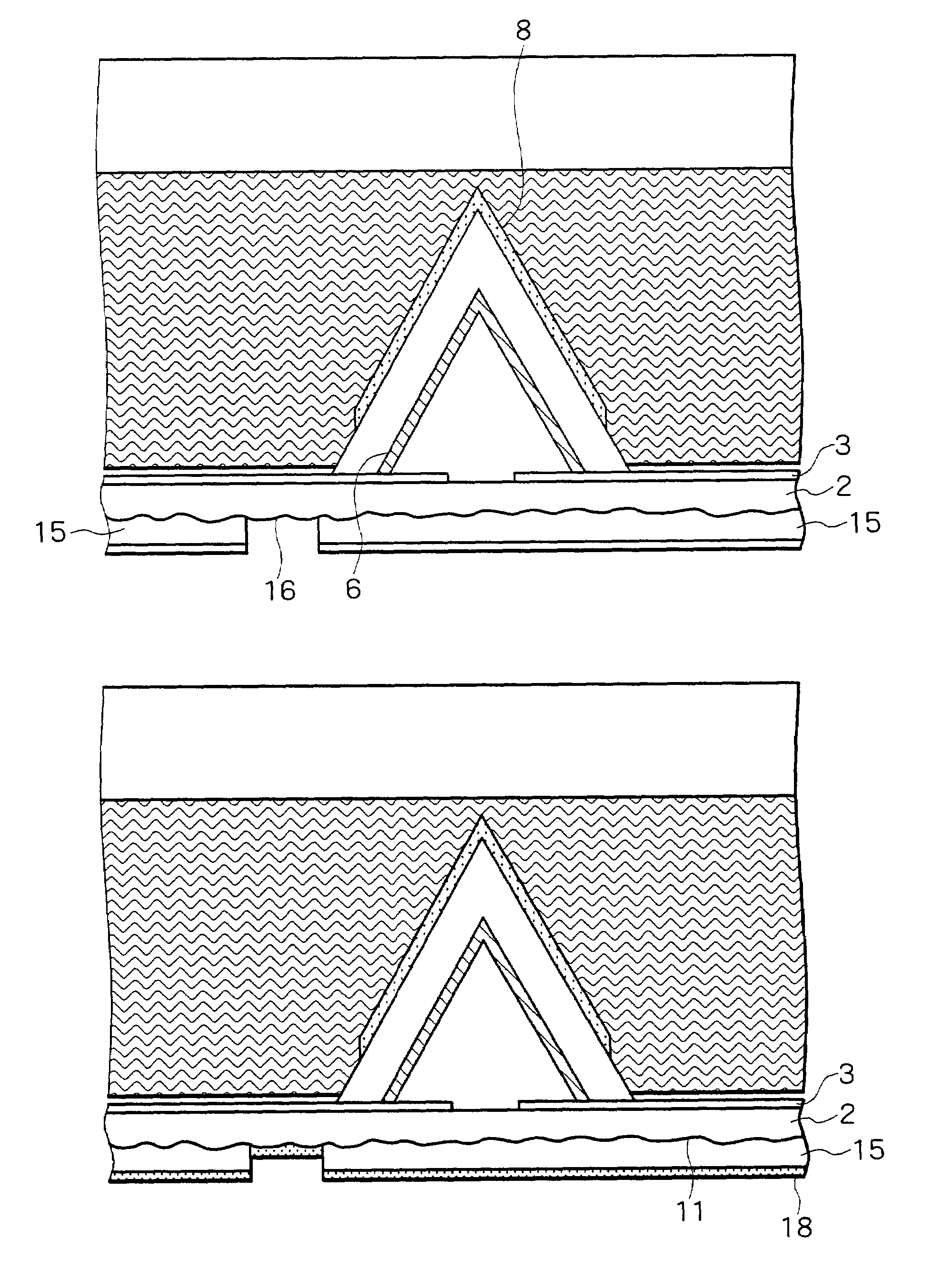
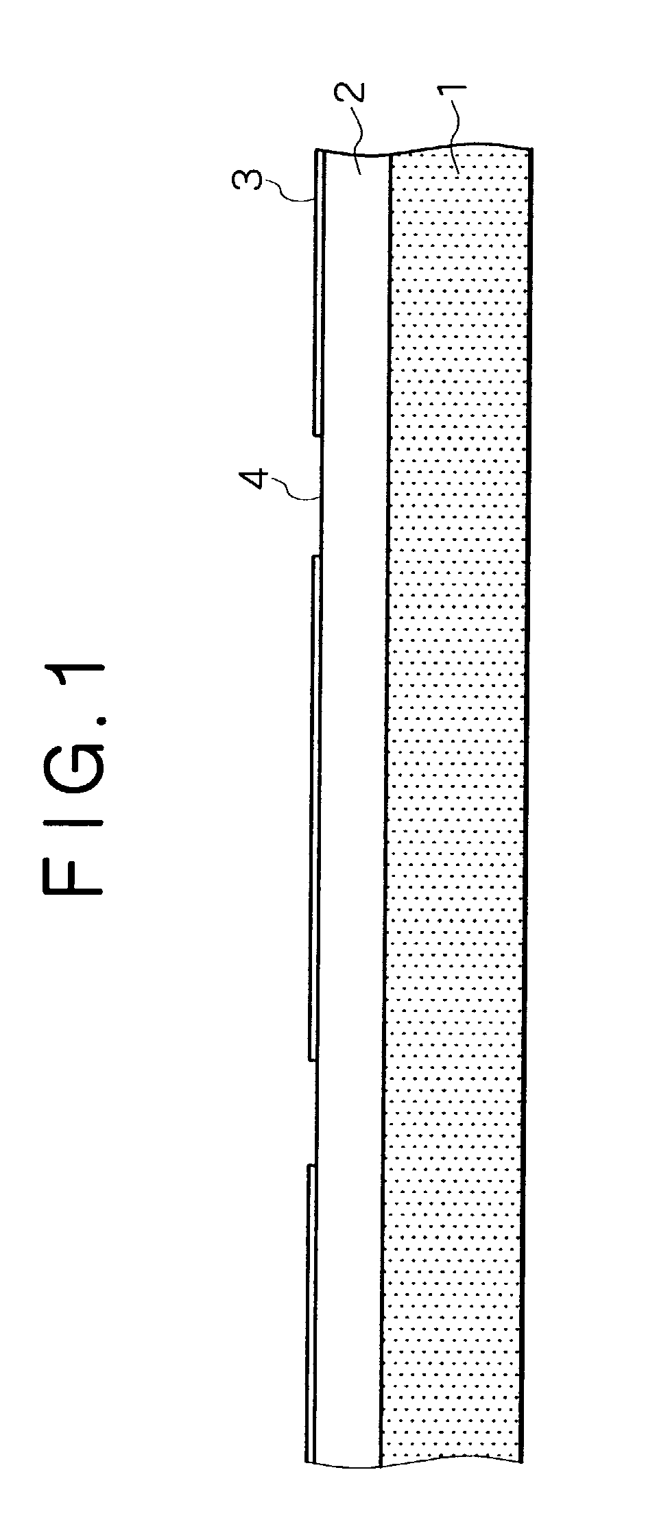
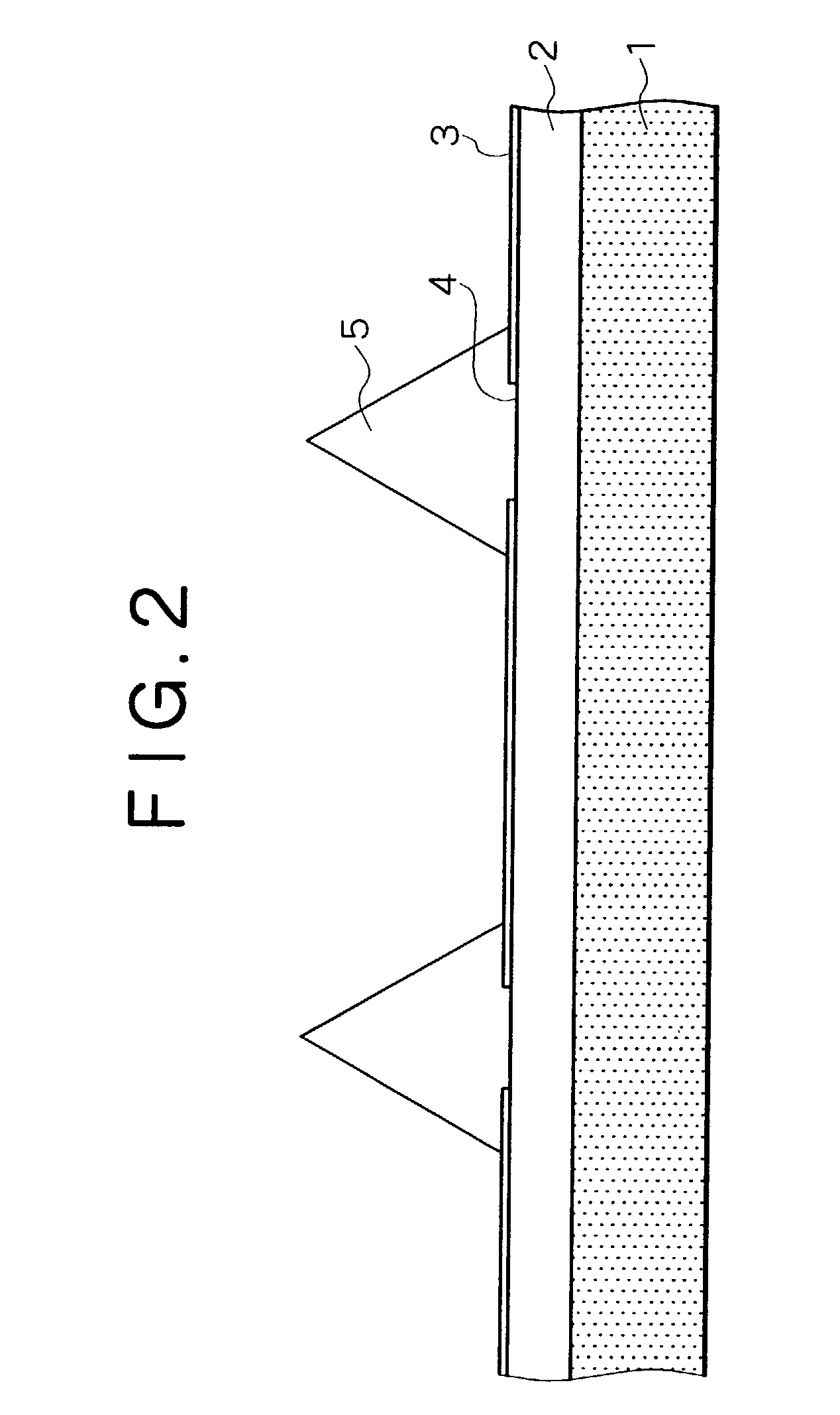
[0056]First, steps of forming a first conductive type layer, an active layer and a second conductive type layer, and forming an electrode on the second conductive type layer, to form a basic structure of each of semiconductor light emitting devices according to the present invention, and the basic structure of the semi-finished light emitting device thus formed will be described with reference to FIGS. 1 to 4.

[0057]A low temperature buffer layer is formed on a principal plane, taken as a (C+)-plane of sapphire, of a sapphire substrate 1. The sapphire substrate 1 is heated to 1000° C., and a silicon-doped GaN layer 2 is formed on the low temperature buffer layer. A mask layer 3 made from SiO2 or SiN is formed to a thickness ranging from 100 nm to 500 nm over the entire surface of the GaN layer 2, and as shown in FIG. 1, window regions 4 composed of circular opening po...

second embodiment

[Second Embodiment]

[0074]A second embodiment of the present invention will be described with reference to FIG. 12. This embodiment relates to another method of forming irregularities using energy beams.

[0075]The method according to this embodiment is effective to more easily form irregularities for a shorter time as compared with the method according to the first embodiment. It is to be noted that steps of forming light emitting devices by crystal growth and peeling a sapphire substrate from a silicon-doped GaN layer of each of the light emitting devices, and a step of forming an n-electrode are the same as those described in the first embodiment. Therefore, the overlapped description thereof is omitted. Also, parts corresponding to those in the first embodiment are denoted by the same reference numerals whereby the overlapped description thereof is omitted as well.

[0076]A projection lens 20 is disposed between a mask 13 not allowing excimer laser beams to pass therethrough and each...

third embodiment

[Third Embodiment]

[0079]A third embodiment of the present invention will be described with reference to FIGS. 13 to 22. In this embodiment, irregularities are previously formed on a principal plane of a substrate, and a crystal layer of a semiconductor light emitting device is grown on the principal plane having the irregularities.

[0080]A sapphire substrate generally used for crystal growth of a nitride semiconductor is used in this embodiment, but it may be replaced with another kind of substrate. For example, a nitride semiconductor substrate can be used as the substrate in this embodiment.

[0081]First, as shown in FIG. 13, irregularities 31 are formed on a principal plane, taken as (C+)-plane of sapphire, of a sapphire substrate 30 by reactive ion etching or by using hydrofluoric acid as an etchant. The irregularities 31 may be formed by polishing the principal plane of the sapphire substrate 30 by using a material having a high hardness such as diamond, to form a number of fine d...


PUM


Abstract

A semiconductor light emitting device includes a crystal growth layer, and a crystal layer composed of a first conductive type layer, an active layer, and a second conductive type layer. The crystal layer is provided on the upper side of the crystal growth layer. In this device, a back plane of the crystal growth layer has irregularities. Since light generated in the device is prevented from being totally reflected from the back plane of the crystal growth layer, the light emergence efficiency of the device can be increased.

Description

BACKGROUND OF THE INVENTION[0001]The present invention relates to a semiconductor light emitting device having a double-hetero structure in which a first conductive type layer, an active layer, and a second conductive type layer are stacked, an image display unit and a lighting apparatus using the semiconductor light emitting device and a method of fabricating the semiconductor light emitting device. In particular, the present invention relates to a semiconductor light emitting device capable of enhancing the light emergence efficiency and a method of fabricating the semiconductor light emitting device.[0002]Various methods have been proposed to enhance luminous of a semiconductor light emitting device. Such methods are mainly classified into a technique of increasing a quantity of light emission generated in a device to an input current of the device, and a technique of increasing a light emergence efficiency; that is, a characteristic to allow light generated in a device to effici...

Claims


Application Information

Patent Timeline
Patent Type & Authority Patents(United States)
IPC IPC(8): H01L29/22H01L33/00H01L21/00H01L33/06H01L33/22H01L33/32H01L33/36
CPCH01L33/22H01L33/24
Inventor OOHATA, TOYOHARUDOI, MASATO
Owner SONY CORP
Why Eureka
Try Eureka