Semiconductor device and method of manufacturing thereof

a technology of semiconductors and semiconductors, applied in the direction of semiconductor devices, electrical devices, transistors, etc., can solve the problems of loss of implanted impurities, oxidation of silicon substrates, and foregoing processes, so as to prevent outward diffusion of impurities, prevent depletion of channels, and excellent characteristics

Inactive Publication Date: 2006-08-29
FUJITSU SEMICON LTD
View PDF10 Cites 9 Cited by
  • Summary
  • Abstract
  • Description
  • Claims
  • Application Information

AI Technical Summary

Benefits of technology

[0021]In the present invention, formation of the gate insulating film and gate electrode is followed by introduction of nitrogen into the surfaces of the semiconductor substrate and gate electrode, so that the areas introduced with nitrogen are successfully prevented from being oxidized even the resist film is formed and then removed thereon. The present invention is also advantageous in that the annealing is carried out in such a state that the surfaces of the semiconductor substrate and gate electrode are introduced with nitrogen, which successfully prevents outward diffusion of impurities already contained therein.
[0022]The present invention is thus successful in preventing depletion of the channel, which has been a problem in the conventional process, and as a consequence in obtaining a semiconductor device having excellent characteristics.

Problems solved by technology

The foregoing process however suffers from a drawback such that the resist films 21, 22 used as the masks when the pocket layers and extension layers are formed must be removed after these layers are formed, where ashing or wet treatment required for removing the resist films 21, 22 inevitably oxidizes the silicon substrate.
Oxidation of the silicon substrate results in loss of the implanted impurities, which fails in attaining an expected concentration and profile.
Oxidation of the silicon substrate is also disadvantageous in that making the extension layers distant from the gate portion to thereby substantially deepen junction of the extension layers.
This undesirably causes degradation of the characteristics, which is typified by short-channel effect.
Another disadvantage of the above-described manufacturing method relates to annealing which is necessary for activating impurities in the source / drain region 15 after the formation thereof, where the annealing undesirably promotes outward diffusion of impurities which reside in the channel to thereby cause depletion of the channel, or undesirably promotes outward diffusion of impurities which reside in the source / drain diffusion region 15.
The oxide film capping, however, suffers from a drawback such that profile of the source / drain diffusion layer becomes deeper due to accelerated diffusion induced by oxygen.
On the other hand, formation of the nitride film having a thickness of 100 nm or around on the side surfaces of the gate electrode by the CVD process tends to result in increased stress and abnormal diffusion.

Method used


Image

  • Semiconductor device and method of manufacturing thereof
  • Semiconductor device and method of manufacturing thereof
  • Semiconductor device and method of manufacturing thereof

Examples


Embodiment Construction

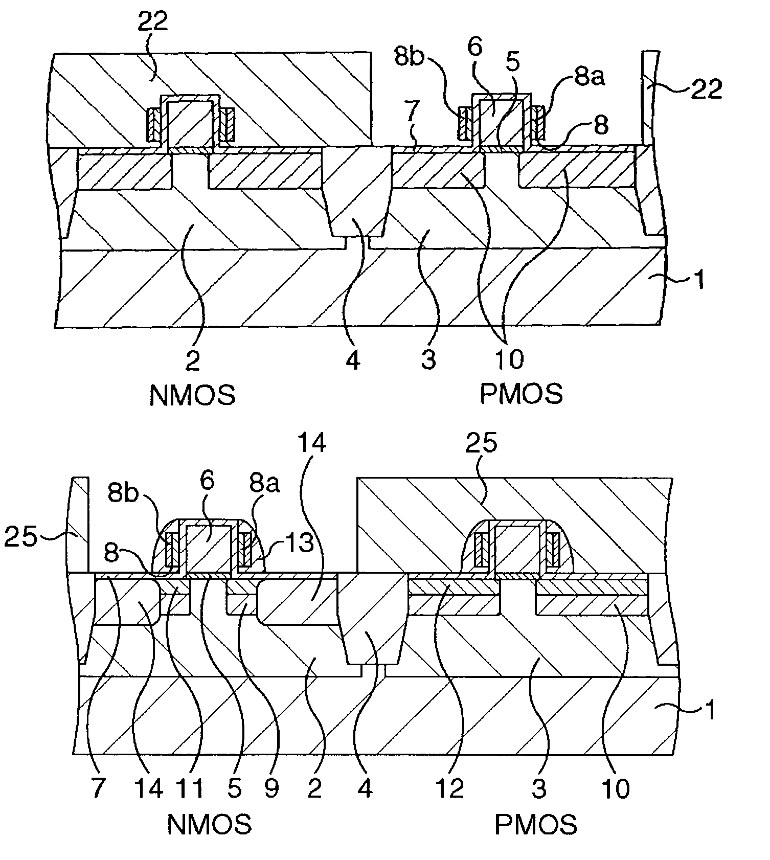
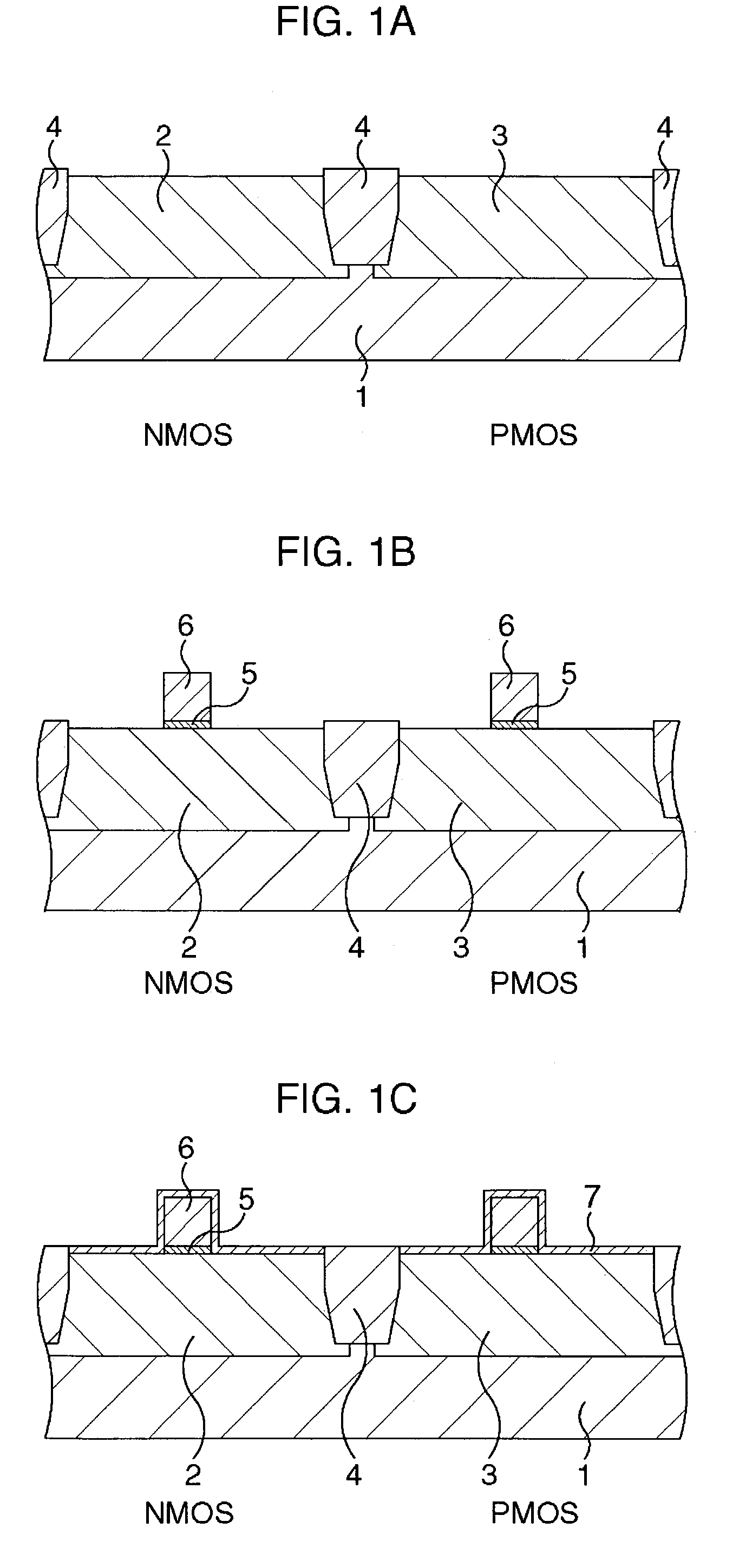
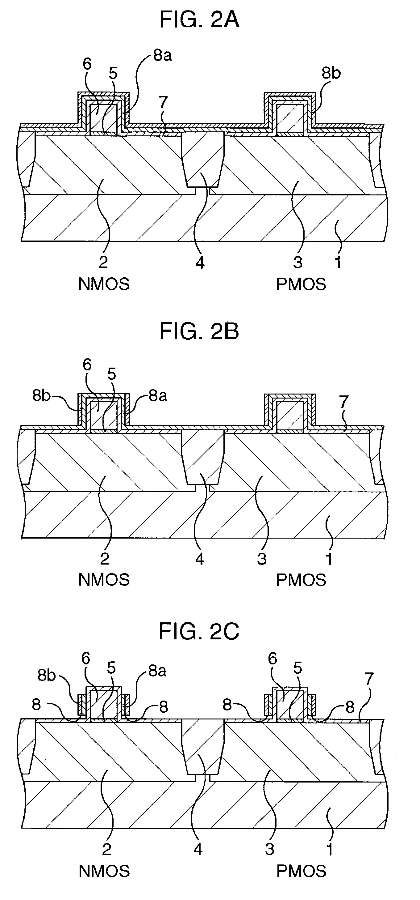
[0041]The semiconductor device and the method of manufacturing thereof according to embodiments of the present invention will specifically be described below. FIGS. 1A through 5C are schematic sectional views serially showing the process steps of the method of manufacturing a semiconductor device according to the first embodiment of the present invention.

[0042]In the first embodiment, an element isolation region 4 is formed in the surficial portion of a P-type semiconductor substrate 1 as shown in FIG. 1A, and wells are then formed in the device forming areas partitioned by the element isolation region 4, where a P-well (channel) 2 is formed in an N-channel MOS (NMOS) area, and an N-well (channel) 3 is formed in a P-channel MOS (PMOS) area.

[0043]Next as shown in FIG. 1B, an insulating film and a polysilicon film are formed on the semiconductor substrate 1, and then patterned to thereby form gate insulating films 5 and gate electrodes 6, respectively, in the device forming areas. The...


PUM

PropertyMeasurementUnit
thicknessaaaaaaaaaa
thicknessaaaaaaaaaa
gas pressureaaaaaaaaaa

Abstract

A silicon nitride film having a thickness of 3 nm or less is formed on the surfaces of a P-well and N-well, as well as on the upper and side surfaces of a gate electrode, in which the silicon nitride film can be formed, for example, by exposing the surface of the P-well and N-well, and the upper and side surfaces of the gate electrode to a nitrogen-gas-containing plasma using a magnetron RIE apparatus. Then, pocket layers, extension layers and source/drain layers are formed while leaving the silicon nitride film unremoved.

Description

CROSS-REFERENCE TO RELATED APPLICATIONS[0001]This application is based upon and claims the benefit of priority from the prior Japanese Patent Application No. 2002-167637, filed on Jun. 7, 2002, the entire contents of which are incorporated herein by reference.BACKGROUND OF THE INVENTION[0002]1. Field of the Invention[0003]The present invention relates to a semiconductor device suitable for composing CMOS (complementary metal-oxide semiconductor) and a method of manufacturing thereof.[0004]2. Description of the Related Art[0005]General procedures for manufacturing conventional CMOS transistor are as follows. FIGS. 15A through 17C are schematic sectional views serially showing process steps of a conventional method of manufacturing a CMOS transistor.[0006]First as shown in FIG. 15A, an element isolation region 4 is formed in the surficial portion of a P-type semiconductor substrate 1, and wells are then formed in the device forming areas partitioned by the element isolation region 4, ...

Claims


Application Information

Patent Timeline
Patent Type & Authority Patents(United States)
IPC IPC(8): H01L21/336H01L21/28H01L21/8238H01L27/092H01L29/78
CPCH01L21/2652H01L21/28247H01L21/823814H01L29/6659H01L21/823857H01L21/823864H01L29/6656H01L21/823828H01L29/42376
Inventor SAIKI, TAKASHI
Owner FUJITSU SEMICON LTD
Why Eureka
Try Eureka