Semiconductor integrated circuit device having logic circuit and dynamic random access memory on the same chip
- Summary
- Abstract
- Description
- Claims
- Application Information
AI Technical Summary
Benefits of technology
Problems solved by technology
Method used
Image

Examples
first embodiment
[0060
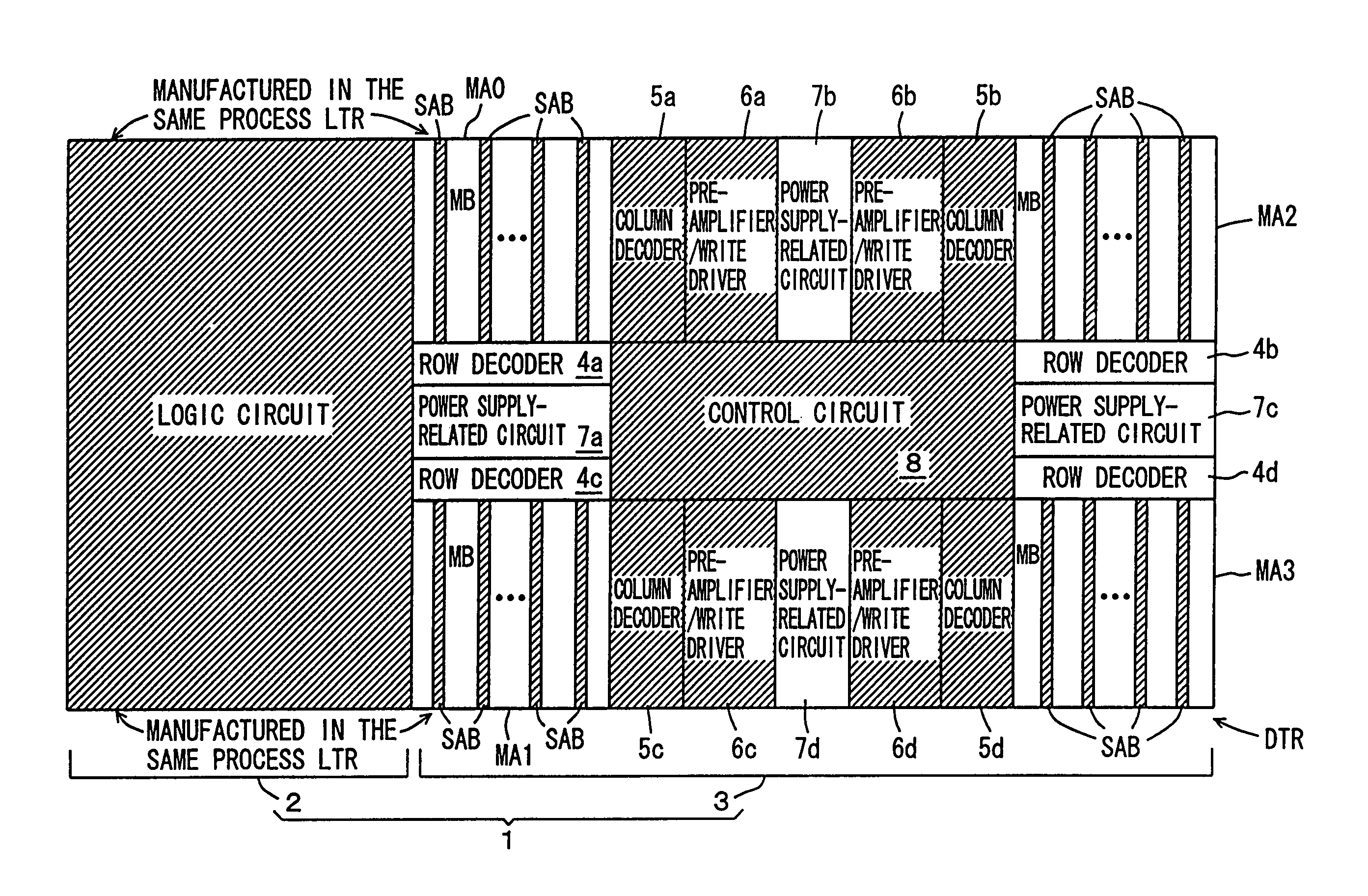
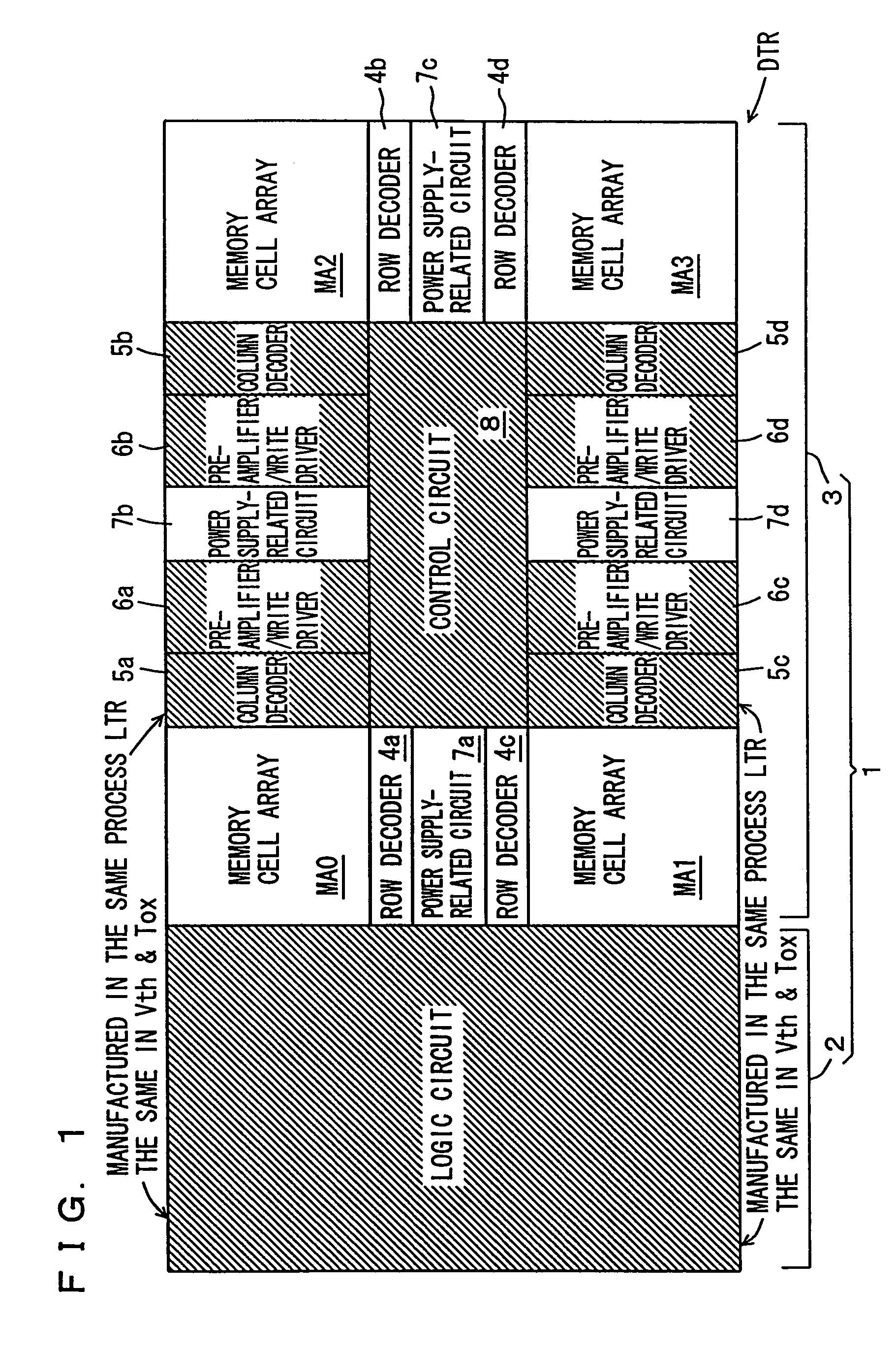
[0061]FIG. 1 is a schematic diagram of an entire configuration of a semiconductor integrated circuit device according to a first embodiment of the present invention. In FIG. 1, semiconductor integrated circuit device 1 includes a logic circuit 2 including as a component of a logic transistor LTR, and a DRAM circuit 3 in which peripheral circuit includes a logic transistor LTR formed in the same manufacturing process as the logic transistor of logic circuit 2.
[0062]DRAM circuit 3 includes memory cell arrays MA0 to MA3 provided in quad-divided regions in the region of DRAM circuit 3 and each having a plurality of memory cells arranged in a matrix of rows and columns, row decoders 4a to 4d provided corresponding to memory cell arrays MA0 to MA3, respectively to drive an addressed row (word line) in a corresponding memory cell array into a selected state, column decoders 5a to 5d provided corresponding to memory cell arrays MA0 to MA3 to generate a column selecting signal for selec...
second embodiment
[0070
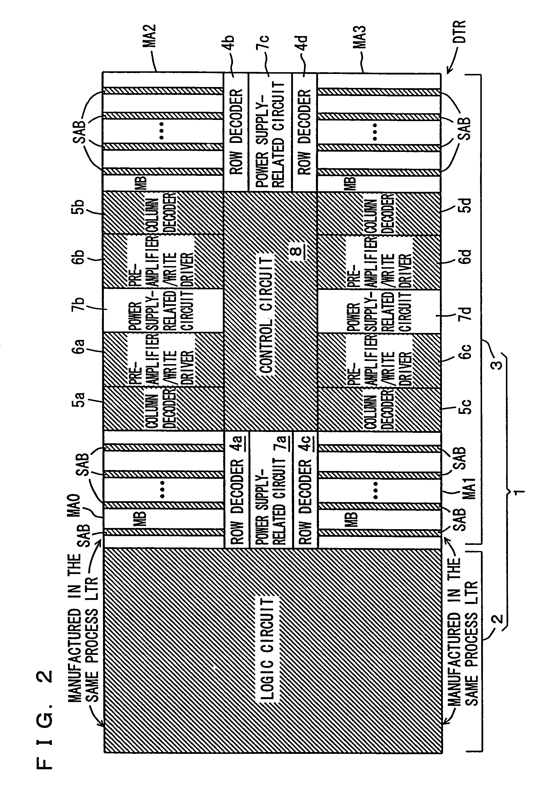
[0071]FIG. 2 is a schematic diagram of an entire general configuration of a semiconductor integrated circuit device according to a second embodiment of the present invention. In semiconductor integrated circuit device 1 shown in FIG. 2, memory cell arrays MA0 to MA3 are each divided into a plurality of memory cell blocks MB by sense amplifier bands SAB extending in the direction along the rows (hereinafter “row direction”). Sense amplifier band SAB includes a sense amplifier circuit provided corresponding to each column of memory cell blocks. The sense amplifier circuit is formed of a MOS transistor formed in the same manufacturing process as logic transistor LTR included in logic circuit 2.
[0072]Column decoders 5a to 5d are provided in common to memory cell blocks MBs included in corresponding memory cell arrays MA0 to MA3. In DRAM circuit 3, 128-bit memory cells for example are selected simultaneously in a column selecting operation in memory cell arrays MA0 to MA3. As a resu...
third embodiment
[0118
[0119]FIG. 10 is a schematic diagram of a main part of a semiconductor integrated circuit device according to a third embodiment of the present invention. In FIG. 10, the configuration of sense amplifier band SAB between 2 memory row blocks MB#a and MB#b are schematically shown. In sense amplifier band SAB, a sense amplifier circuit group SKG including a sense amplifier circuit provided corresponding to each bit line pair of memory row blocks MB#a and MB#b is provided. The source nodes of the sense amplifier circuit included in sense amplifier circuit group SKG are coupled to a P drive signal line S2P and an N drive signal line S2N, respectively.
[0120]Sense (array) power supply line Vccs and sense ground line Vss are formed in parallel to P drive signal line S2P and N drive signal line S2N.
[0121]In the crossing regions of the sense amplifier band sub decoder bands SWD#0 to SWD#q between memory sub arrays adjacent in the row direction, P-channel MOS transistors PSD0 to PSDq to c...
PUM
 Abstract
Description
Claims
Application Information
 - Generate Ideas
- Intellectual Property
- Life Sciences
- Materials
- Tech Scout
- Unparalleled Data Quality
- Higher Quality Content
- 60% Fewer Hallucinations
Browse by: Latest US Patents, China's latest patents, Technical Efficacy Thesaurus, Application Domain, Technology Topic, Popular Technical Reports.
© 2025 PatSnap. All rights reserved.Legal|Privacy policy|Modern Slavery Act Transparency Statement|Sitemap|About US| Contact US: help@patsnap.com