Semiconductor device and a method of manufacturing the same

a technology of semiconductor devices and semiconductors, applied in the direction of semiconductor devices, electrical devices, transistors, etc., can solve problems such as process-induced residual stress in elements, and achieve the effect of suppressing the effect of short channel effects

Inactive Publication Date: 2006-09-12
RENESAS ELECTRONICS CORP
View PDF12 Cites 101 Cited by
  • Summary
  • Abstract
  • Description
  • Claims
  • Application Information

AI Technical Summary

Benefits of technology

[0006]In the ordinarily employed CMIS (complementary MIS) process, the material used for the formation of an interlayer insulating film over the circuit formation surface of a semiconductor substrate is not different between the n-channel conductivity type MISFET and p-channel conductivity type MISFET. As a result, their stresses working on the channel formation region are substantially equal in one chip. It is the common practice to make a process-wise device in order to reduce the stress working on the channel formation regions of the n-channel conductivity type MISFET and p-channel conductivity type MISFET.
[0016]Therefore, it is an object of the present invention to provide a technique that is capable of increasing the drain current of each of the n-channel conductivity type MISFET and p-channel conductivity type MISFET (increasing the current driving capacity).
[0017]Another object of the present invention is to provide a technique that enables free setting of a drain current ratio between the n-channel conductivity type MISFET relative to that of the p-channel conductivity type MISFET.
[0094]The stresses working on the channel formation regions of the n-channel conductivity type field effect transistor and p-channel conductivity type field effect transistor, respectively, make it possible to freely control the drain current ratio of the n-channel conductivity type field effect transistor relative to the p-channel conductivity type field effect transistor.

Problems solved by technology

This tends to leave a process-induced residual stress in the element.

Method used


Image

  • Semiconductor device and a method of manufacturing the same
  • Semiconductor device and a method of manufacturing the same
  • Semiconductor device and a method of manufacturing the same

Examples


embodiment 1

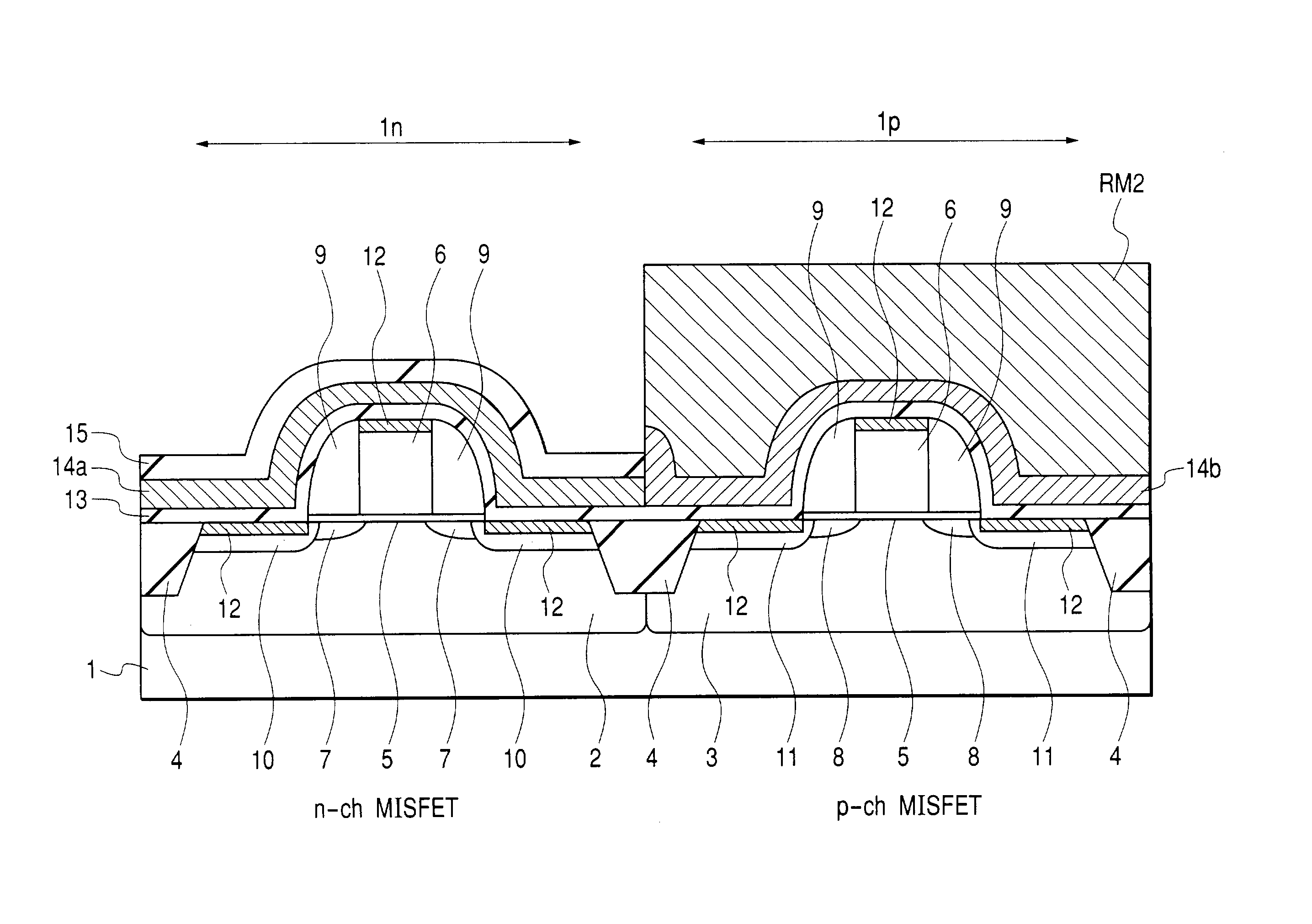
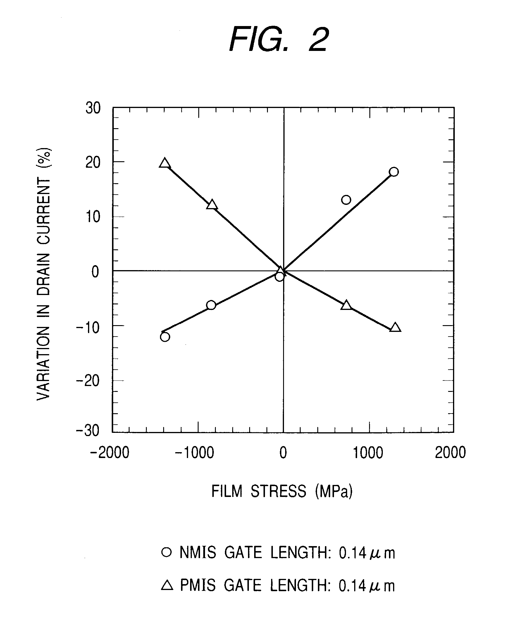
[0155]In Embodiment 1, application of the present invention to a semiconductor device having a complementary MISFET structure and having a power-supply voltage of from 1 to 1.5V and a gate length of from 0.1 to 0.14 μm will be described.

[0156]In FIG. 1 and FIGS. 5 to 19, an n channel conductivity type MISFET (n-type MISFET) is illustrated on the left side, while a p channel conductivity type MISFET (p-type MISFET) is illustrated on the right side.

[0157]As illustrated in FIG. 1, the semiconductor device according to this Embodiment has a semiconductor substrate composed mainly of a p type silicon substrate (which will hereinafter simply be called a “p type substrate”) made of, for example, single crystal silicon. The circuit formation surface (one main surface) of the p type substrate 1 has thereon an nMIS formation region (first element formation region) 1n and a pMIS formation region (second element formation region) 1p, and the nMIS formation region 1n is separated from the pMIS f...

embodiment 2

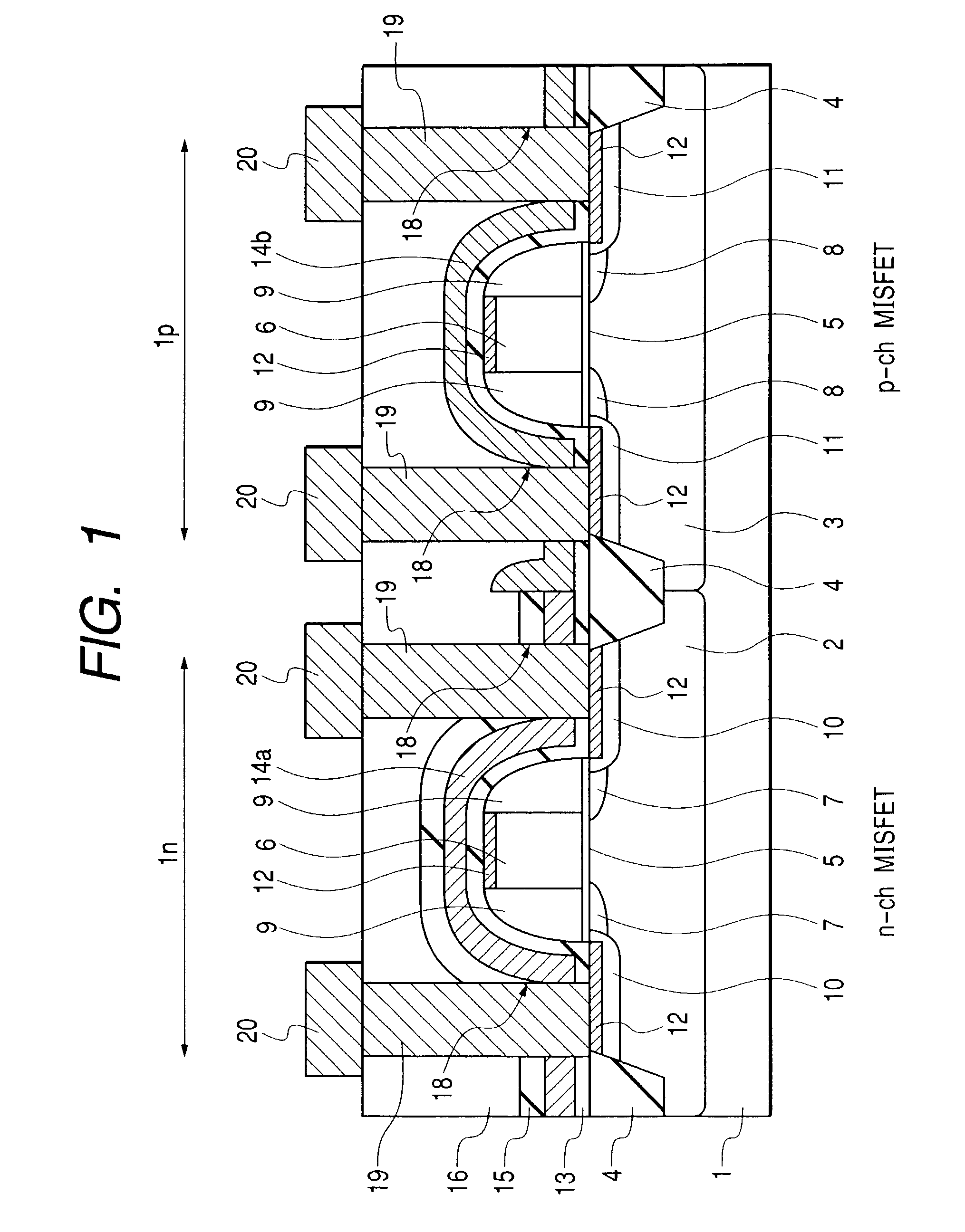
[0234]FIG. 25 is a schematic cross-sectional view illustrating the rough constitution of a semiconductor device according to Embodiment 2 of the present invention.

[0235]FIGS. 26A, 26B and 27 are each a schematic cross-sectional view of the semiconductor device, at a manufacturing step thereof, according to Embodiment 2 of the present invention. In FIGS. 25 to 27, an n-type MISFET is illustrated on the lift side, while a p-type MISFET is illustrated on the right side.

[0236]As illustrated in FIG. 25, the semiconductor device of Embodiment 2 is similar to that of Embodiment 1 except that the insulating film 13 serving as an etching stopper is removed.

[0237]When the insulating film 13 is left as in Embodiment 1 (refer to FIG. 18), the stress of the silicon nitride films (14a, 14b) concentrates on the foot of the step portion 35a, that is defined by the gate electrode 6, sidewall spacers 9 and insulating film 13, and the starting point of the stress of the silicon nitride films (14a, 14b...

embodiment 3

[0243]FIG. 28 is a schematic cross-sectional view of a semiconductor device, at a manufacturing step thereof, according to Embodiment 3 of the present invention. In FIG. 28, the left side illustrates an n-type MISFET, while the right side illustrates a p-type MISFET.

[0244]In Embodiment 1, the insulating film 13 made of a silicon oxide film formed by the deposition method was used as an etching stopper upon removal of the silicon nitride film 14a. In Embodiment 3, on the other hand, an insulating film 21, made of a silicon oxide film formed by the thermal oxidation method, is used as an etching stopper upon removal of the silicon nitride film 14a. The formation of the insulating film 21 by the thermal oxidation method is conducted after the step of forming the n-type and p-type MISFETs having a salicide structure, but before the step of forming the silicon nitride films 14a, 14b.

[0245]By the thermal oxidation method, the insulating film 21 can be formed selectively so as to cover th...


PUM


Abstract

A method of manufacturing a semiconductor device having an n-type FET and p-type FET, each formed over a semiconductor substrate, calls for (a) forming, over the n-type FET and p-type FET, a first insulating film, for generating a tensile stress in the channel formation region of the n-type FET, to cover gate electrodes of the FETs, while covering, with an insulating film, a semiconductor region between the gate electrode of the p-type FET and an element isolation region of the semiconductor substrate; (b) selectively removing the first insulating film from the upper surface of the p-type FET by etching; (c) forming, over the n-type and p-type FETs, a second insulating film, for generating a compressive stress in the channel formation region of the p-type FET, to cover gate electrodes of the FETs; and (d) selectively removing the second insulating film from the upper surface of the n-type FET.

Description

TECHNICAL FIELD[0001]The present invention relates to a semiconductor device and to a method of manufacture thereof; and, more particularly, the invention relates to a semiconductor device having, on the same substrate thereof, both an n-channel conductivity type field effect transistor and a p-channel conductivity type field effect transistor, and to a technique that is effective when applied to the manufacture of such a semiconductor device.BACKGROUND OF THE INVENTION[0002]One example of a field effect transistor installed on a semiconductor device is an insulated gate field effect transistor called a “MISFET” (Metal Insulator Semiconductor Field Effect Transistor). Owing to the characteristics of this MISFET that allow it to be readily applicable to high integration, it has been used widely as a circuit element constituting an integrated circuit.[0003]Irrespective of whether it is of an n-channel conductivity type or p-channel conductivity type, a MISFET usually has a channel for...

Claims


Application Information

Patent Timeline
Patent Type & Authority Patents(United States)
IPC IPC(8): H01L21/336H01L21/8234H01L29/78H01L21/8238H01L27/092
CPCH01L21/823807H01L21/823828H01L29/7843H01L29/665H01L29/78645H01L29/785H01L29/78642H01L21/8234
Inventor HACHIMINE, KIYOTASHIMIZU, AKIHIROOOKI, NAGATOSHISAKAI, SATOSHIYAMAMOTO, NAOKI
Owner RENESAS ELECTRONICS CORP
Why Eureka
Try Eureka