Method and device for polishing

a technology of nitride film and polishing method, which is applied in the direction of polishing compositions, abrasive surface conditioning devices, lapping machines, etc., can solve the problems of process inability to eliminate dishing completely, insufficient uniformity of within-wafers, and impaired subsequent etching of nitride films, so as to reduce the polishing rate of nitride films, less likely to cause dishing, and flatter finished surfaces

Inactive Publication Date: 2006-09-19
EBARA CORP
View PDF18 Cites 17 Cited by
  • Summary
  • Abstract
  • Description
  • Claims
  • Application Information

AI Technical Summary

Benefits of technology

[0013]The present invention has been made in view of the above problems in the prior art. It is therefore an object of the present invention to provide a polishing method and a polishing apparatus which can suppress dishing in a workpiece having a nitride film and an oxide film formed on the nitride film, and obtain within-wafer uniformity.
[0017]In a neutral to acidic pH region of the polishing liquid, surfaces of abrasive particles of the fixed abrasive and the surface of the nitride film are principally charged positively (though part of the surfaces possess a negative charge, a positive charge is predominant). Accordingly, the anionic surface-active agent supplied onto the fixed abrasive strongly adheres to the surfaces of the abrasive particles of the fixed abrasive and to the surface of the nitride film electrically. Since the abrasive particles of the fixed abrasive and the nitride film are both covered with the anionic surface-active agent they interact repulsively. Therefore, polishing of the nitride film is hard to proceed and a polishing rate of the nitride film becomes extremely low. The polishing selectivity is, for example, oxide film:nitride film=10 or higher: 1, and the nitride film acts as a polishing stopper. Since the polishing rate of the nitride film is extremely lowered and stock removal decreases, a resulting nitride film can be prevented from becoming uneven in terms of film thickness and within-wafer uniformity of the nitride film can be obtained.
[0019]① The anionic surface-active agent adheres not only to the surface of the nitride film, but also to the silicon oxide film in a small amount, whereby a coat of the anionic surface-active agent is formed on the surface of the silicon oxide film. When a surface pressure having at least a certain value is applied to the silicon oxide, a coat on the surface of the silicon oxide film breaks or becomes fragile, and therefore polishing of the silicon oxide film proceeds. As the polishing proceeds to a certain extent, however, a level of the surface of the silicon oxide film becomes lower than that of the nitride film. Accordingly, the surface pressure on the silicon oxide film decreases, and hence a thick coat of the anionic surface-active agent is formed on the silicon oxide film and progress of polishing is retarded.
[0021]Further, the present invention uses a fixed abrasive as a polishing surface. A fixed abrasive provides a hard polishing surface which hardly deforms elastically. Such a polishing surface, as compared to a conventional polishing pad having elasticity, is less likely to cause dishing and can provide a flatter finished surface. However, if a hard polishing pad which has a hardness equivalent to a fixed abrasive is used, then the polishing pad, a slurry, and a surface-active agent may be used.
[0022]Thus, according to the present invention, polishing of a workpiece is performed while supplying the polishing liquid which contains an anionic surface-active agent and does not contain abrasive particles, onto the fixed abrasive, whereby a nitride film, for example, is allowed to act as a polishing stopper. Accordingly, the polishing method of the present invention can lower a polishing rate of a nitride film to obtain within-wafer uniformity of the nitride film and can suppress dishing, thus enabling a high-flatness polishing with fewer scratches.

Problems solved by technology

If the excessive silicon oxide film is not removed completely, then subsequent etching of the nitride film will be impaired.
Furthermore, the nitride film tends to be polished unevenly, resulting in insufficient within-wafer uniformity.
However, this process cannot eliminate dishing completely because it also uses a soft polishing pad.
Another problem of this process is that the high concentration surface-active agent causes ceria to agglomerate, and this agglomerated ceria scratches the wafer.
However, the publication refers to nothing about optimization of the polishing process which includes multi-stage polishing, dressing, and post-processing.

Method used


Image

  • Method and device for polishing
  • Method and device for polishing
  • Method and device for polishing

Examples


Embodiment Construction

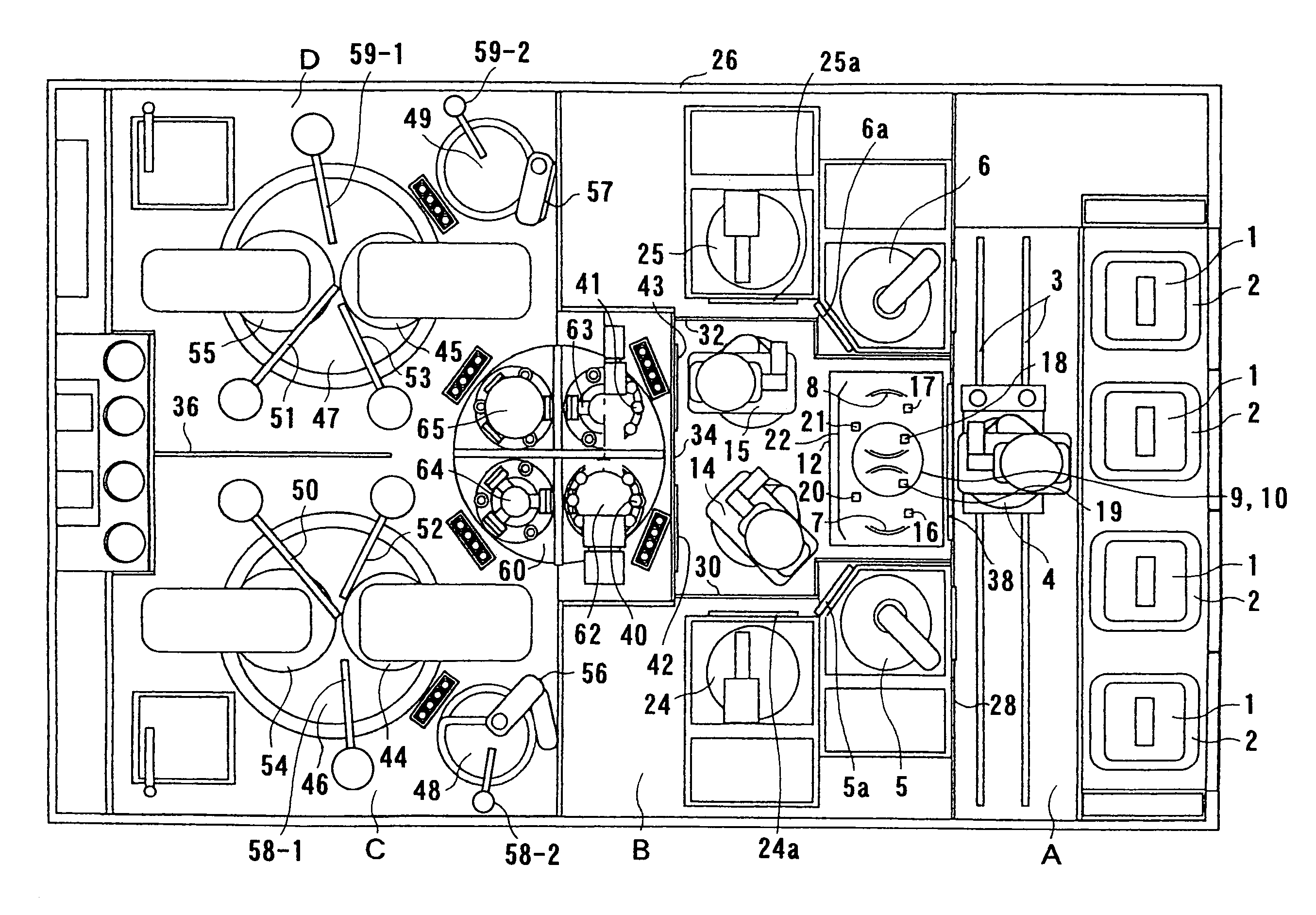
[0035]A polishing apparatus according to embodiments of the present invention will be described in detail below with reference to the drawings. FIG. 1 is a plan view showing an entire arrangement of a polishing apparatus according to an embodiment of the present invention.

[0036]As shown in FIG. 1, the polishing apparatus comprises four load / unload stages 2 each for receiving a wafer cassette 1 which accommodates a number of semiconductor wafers. The load / unload stages 2 may have a lifting and lowering mechanism. A transfer robot 4 is provided on rails 3 so that the transfer robot 4 can access respective wafer cassettes 1 on respective load / unload stages 2.

[0037]The transfer robot 4 has upper and lower hands. The lower hand of the transfer robot 4 is a vacuum attraction-type hand for holding a semiconductor wafer under vacuum, and is used only for removing a semiconductor wafer from a wafer cassette 1. The vacuum attraction-type hand can hold and transport the semiconductor wafer eve...


PUM

PropertyMeasurementUnit
thicknessaaaaaaaaaa
thicknessaaaaaaaaaa
angleaaaaaaaaaa

Abstract

The present invention relates to a polishing method for polishing a workpiece by pressing the workpiece, to be polished, against a fixed abrasive and bringing the workpiece into sliding contact with the fixed abrasive. The polishing method includes a first step of polishing the workpiece while supplying a polishing liquid which contains an anionic surface-active agent and does not contain abrasive particles, and a second step of polishing the workpiece while supplying a polishing liquid which contains a cationic surface-active agent and does not contain abrasive particles.

Description

[0001]This application is a National Stage application of PCT / JP03 / 01869, filed Feb. 20, 2003.[0002]1. Technical Field[0003]The present invention relates to a polishing method and apparatus, and more particularly to a polishing method and apparatus for polishing a workpiece such as a semiconductor wafer with a fixed abrasive.[0004]2. Background Art[0005]As semiconductor devices have become more highly integrated in recent years, circuit interconnections have become finer and distance between those circuit interconnections becomes smaller. In case of photolithography which can form interconnections that are at most 0.5 μm wide, it is required that surfaces on which pattern images are to be focused by a stepper should be as flat as possible because a depth of focus of an optical system is relatively small. A polishing apparatus for performing chemical mechanical polishing (CMP) has been used for planarizing a semiconductor wafer.[0006]This type of chemical mechanical polishing (CMP) a...

Claims


Application Information

Patent Timeline
Patent Type & Authority Patents(United States)
IPC IPC(8): B24B49/00B24B1/00B24B7/22B24B37/04B24B49/12B24B53/007B24B53/02C09G1/00H01L21/304H01L21/3105
CPCB24B7/228B24B37/04B24B37/044H01L21/31053B24B53/017B24B53/02C09G1/00B24B49/12
Inventor WADA, YUTAKAAKATSUKA, TOMOHIKOSASAKI, TATSUYA
Owner EBARA CORP
Why Eureka
Try Eureka