Micro defects in semi-conductors

a technology of semi-conductors and defects, applied in semiconductor/solid-state device testing/measurement, optical radiation measurement, fluorescence/phosphorescence, etc., can solve problems such as yield loss and reliability problems, device failure, and dislocation free wafers may not be able to remain this way

Inactive Publication Date: 2006-09-26
NANOMETRICS
View PDF5 Cites 72 Cited by
  • Summary
  • Abstract
  • Description
  • Claims
  • Application Information

AI Technical Summary

Benefits of technology

[0007]However, our investigations have lead us to develop a PL technique which has industrial application in that it enables the image to be produced within minutes. Moreover, our technique also has a further added advantage in that we are able to obtain a micro image of small individual defects near to the surface of the wafer; this is in contrast to the aforementioned PL room temperature technique which tends to produce a macro view of large defect clusters deep into the wafer.

Problems solved by technology

However, dislocation free wafers may not be able to remain this way after the wafers are subjected to high temperature processing.
Defects formed within the device active region in the wafer and defects produced in the gate oxide generally degrade device performance, lead to yield losses and reliability problems.
Transition metals, which are fast diffusers in silicon, readily form deep levels, ie away from the valance or conduction band edge, and also lead to decoration of both point and extended defects which eventually lead to device failure.
Thus internal gettering techniques introduce defects in the silicon substrate which attract unwanted impurities away from the device areas.
However it is not always possible to use an epitaxial layer of sufficient thickness for this activity and where the epitaxial layer is thin then defects in the bulk wafer can interfere with the electrical device.
Moreover, epitaxial layers suffer from problems of metal contamination.
However they do not measure the electrical properties of the defects and moreover in some cases they are destructive.
Accordingly, as techniques for determining the structural integrity of a wafer they are lacking in terms of the information they provide and moreover they can be positively destructive.
However, in all these applications in order to obtain this spectral information and unambiguous chemical identification of the optical centres, measurements need to be carried out at liquid helium temperatures.
It is known throughout the industry that at room temperature the PL signal is significantly weakened and very little useful spectral information can be obtained.
This effectively limits the successful use of this technology.

Method used


Image

  • Micro defects in semi-conductors
  • Micro defects in semi-conductors
  • Micro defects in semi-conductors

Examples


Embodiment Construction

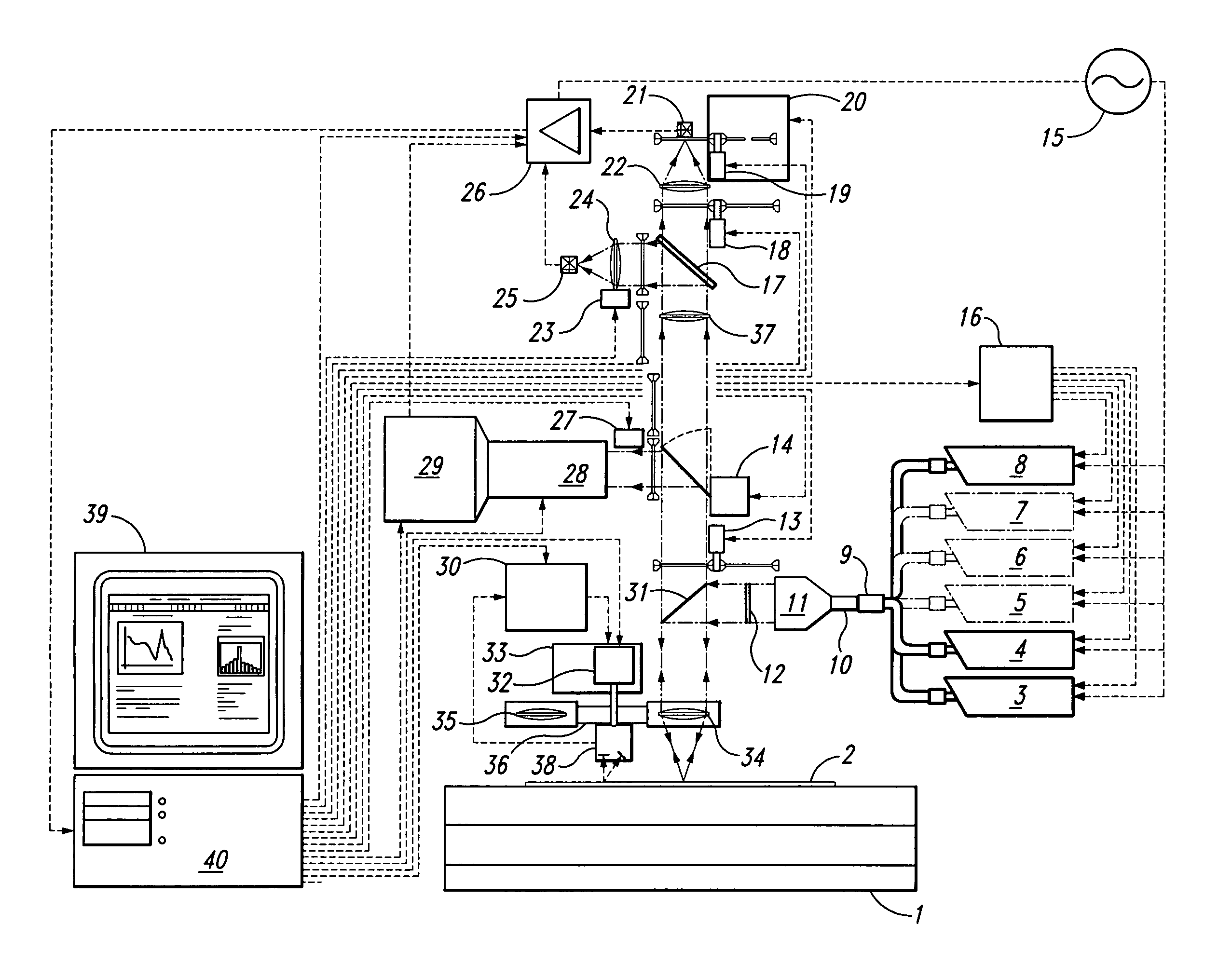
[0047]Referring to the figures and firstly to FIG. 9 there is shown a diagrammatic illustration of an apparatus in accordance with the invention.

[0048]The apparatus essentially comprises a PL imaging microscope which: towards the right hand side, comprises a bank of lasers 3–8; towards the bottom comprises a sample stage such as an X-Y table or R-Θ table; towards the left hand side comprises a microprocessor 40 and a display screen 39 and in the centre of the Figure there are shown various optical components for directing light through the system.

[0049]In the embodiment shown in FIG. 9, six lasers are provided with a view to probing different depths in the sample. However, it is within the scope of the invention to use only one laser, or indeed to use a greater number of lasers. In any event, at least one of the lasers is a high intensity laser and ideally has a spot size of between 0.1 mm and 0.5 micron and a power density of between 104 to 109 watts / cm2. A laser selector 16 couple...


PUM

PropertyMeasurementUnit
sizeaaaaaaaaaa
sizeaaaaaaaaaa
wavelengthsaaaaaaaaaa

Abstract

The invention relates to a method and apparatus for detecting defects in a semiconductor or silicon structure at room temperature, and in an efficient time, using photoluminescence. The invention employs the use of a high intensity beam of light preferably having a spot size between 0.1 mm–0.5 microns and a peak or average power density of 104–109 w / cm2 with a view to generating a high concentration of charge carriers, which charge characters detect defects in a semiconductor by interacting with same. These defects are visible by producing a photoluminescence image of the semiconductor. Several wavelengths may be selected to identify defects at a selective depth as well as confocal optics may be used.

Description

BACKGROUND OF THE INVENTION[0001]The invention relates to an apparatus and method for detecting micro defects in semiconductors or silicon and particularly, but not exclusively, in part-processed or bulk silicon.[0002]Developments in crystal growth have enabled the production of silicon wafers free from dislocation. However, dislocation free wafers may not be able to remain this way after the wafers are subjected to high temperature processing. Defects formed within the device active region in the wafer and defects produced in the gate oxide generally degrade device performance, lead to yield losses and reliability problems. This invention can be used to locate and measure the electrical activity of these defects.[0003]Transition metals, which are fast diffusers in silicon, readily form deep levels, ie away from the valance or conduction band edge, and also lead to decoration of both point and extended defects which eventually lead to device failure. These transition metal impuritie...

Claims


Application Information

Patent Timeline
Patent Type & Authority Patents(United States)
IPC IPC(8): G01J3/30G01J3/00H01L21/00G01N21/64G01N21/88G02B21/00H01L21/66
CPCG01N21/6489G01N21/64
Inventor HIGGS, VICTORMAYES, IAN CHRISTOPHERYUN HENG CHIN, FREDDIESWEENEY, MICHAEL
Owner NANOMETRICS
Why Eureka
Try Eureka