High voltage ripple reduction and substrate protection

Inactive Publication Date: 2006-10-03
SANDISK TECH LLC
View PDF31 Cites 38 Cited by
  • Summary
  • Abstract
  • Description
  • Claims
  • Application Information

AI Technical Summary

Benefits of technology

[0014]Accordingly, it is a general object of the present invention to provide a charge pump with ripple reduction capability. In particular, it is an object to provide a charge pump for s

Problems solved by technology

Conventional mass storage, based on rotating magnetic medium such as hard drives and floppy disks, is unsuitable for the mobile and handheld environment.
This is because disk drives tend to be bulky, are prone to mechanical failure and have high latency and high power requirements.
These undesirable attributes make disk-based storage impractical in most mobile and portable applications.
Fluctuations in the applied voltage m

Method used


Image

  • High voltage ripple reduction and substrate protection
  • High voltage ripple reduction and substrate protection
  • High voltage ripple reduction and substrate protection

Examples


first embodiment

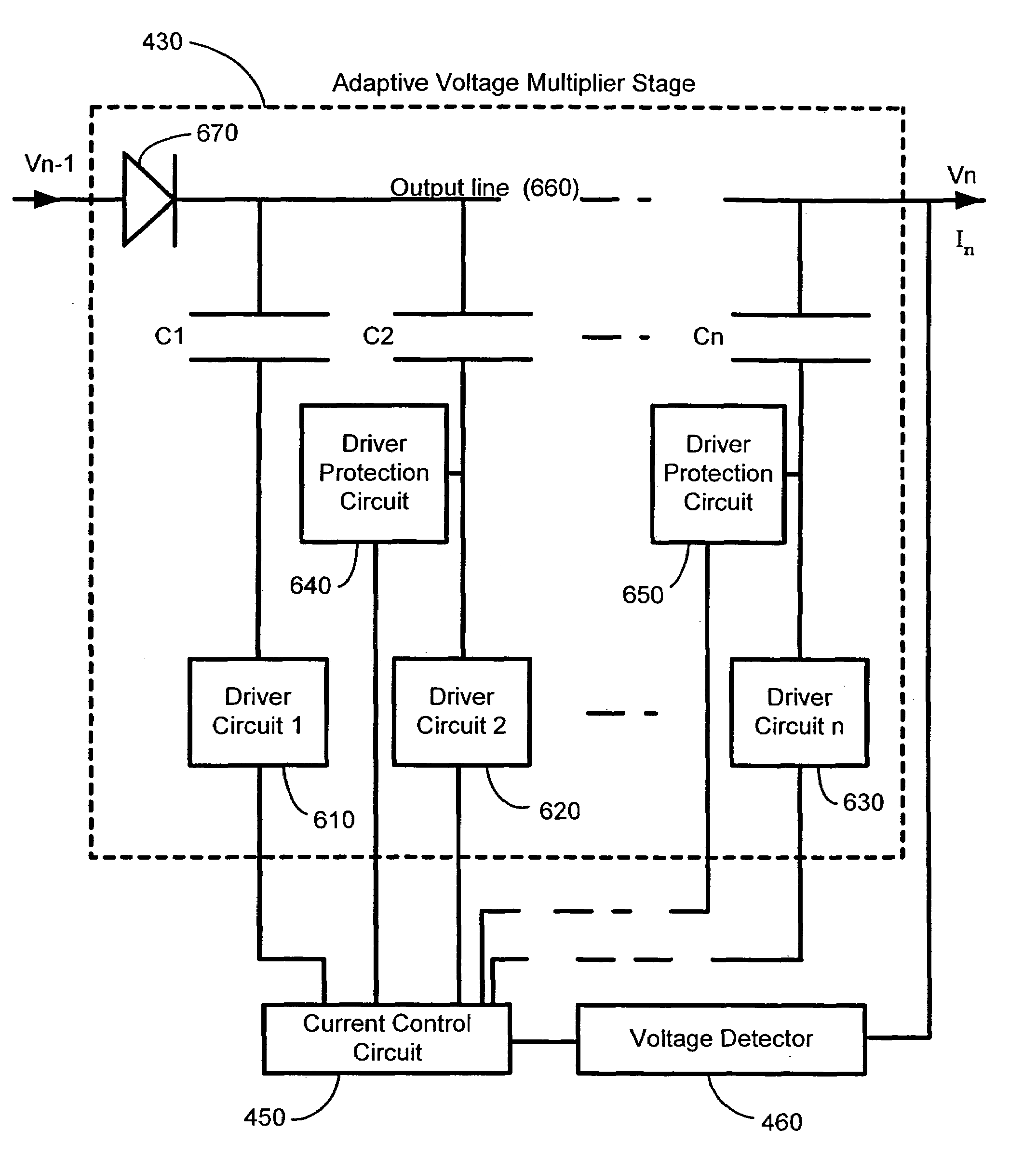
[0037]FIG. 6 illustrates schematically the present invention. This is an adaptive voltage multiplier stage 430 with controlled current output. This stage has a diode 670 and several capacitors C1–Cn connected in parallel instead of the single capacitor C of the prior art shown in FIG. 2. Each capacitor C1–Cn has a corresponding driver circuit 610–630. These capacitors may be enabled or disabled by the current control circuit 450 in response to a signal from the voltage detector 460. Enabled capacitors operate like the capacitor C of FIG. 2. Disabled capacitors are no longer active in the voltage multiplier stage. By disabling capacitors, the capacitance used in the adaptive voltage multiplier stage may be reduced. This reduces the charge stored according to the equation: Q=CV. With less charge stored, less charge is pumped from the stage on each clock cycle. The result is less charge pumped per unit time, that is, less current output.

[0038]Drivers for disabled capacitors do not supp...

second embodiment

[0040]FIG. 7 illustrates the present invention. This embodiment provides a second means to control the current output by using an adaptive driver circuit 700. This may be used in place of the driver circuit shown in FIG. 2, or driver circuit 1610 of FIG. 6. This is a driver circuit that has two possible levels of output voltage. The voltage supply, Vcc, goes to two transistors, T1 and T2. The first transistor, T1, is configured to provide a high voltage (approximately Vcc) at node N1. Transistor T1 is controlled by the current control circuit 450. It is turned on in mode 1, and turned off in mode 2. The second transistor, T2, is configured to provide a lower voltage at node N1 when T1 is turned off. The gate of T2 is controlled by the clamp regulation circuit 710 to provide a constant, low voltage at N1. This, in turn, lowers the output of the driver circuit. The effect of providing a lower voltage to the capacitor is to drive less charge through the stage on each clock cycle. There...

third embodiment

[0043]FIG. 9 illustrates a driver circuit of the This is a switchable adaptive driver circuit 900. This may be used as driver circuit 2–-driver circuit n (620–630) in FIG. 6. This circuit is similar to the adaptive driver circuit 700 shown in FIG. 7. It has two parallel voltage supplies from Vcc. One branch is controlled by the current control circuit 450 to provide a high voltage output in mode 1. The other branch is regulated by the clamp regulation circuit 710 to provide a reduced voltage output in mode 2. However the transistors in this circuit are arranged so that T7 and T8 are directly connected to the driver output. The driver output is susceptible to voltages coupled through the capacitor when the capacitor is disabled. Transistors T7, T8 and T9 are all N-channel devices and so only N-channel devices are directly connected to the driver output in this configuration. This allows the driver output voltage to be held at a particular voltage level that is selected to reduce the...


PUM


Abstract

In a non-volatile memory, charge pumps are used to provide high voltages needed for programming memory cells that have floating gate structures. Charge pumps have a series of voltage multiplier stages in series to boost voltage. These charge pumps must rapidly charge a load to a high voltage and then maintain a voltage with a high degree of stability. Techniques for achieving both of these goals are presented. In one aspect, a charge pump has two operating states, one to charge a load rapidly and a second to maintain a voltage on a charged load with high stability. These states are achieved by changing the current output-from a high current during charging to a low current to maintain the voltage. This is done by changing the capacitance used in the individual voltage multiplier stages. In another aspect, two different current levels are produced by changing the voltage used to charge the capacitors of the voltage multiplier stages.

Description

CROSS-REFERENCE TO RELATED APPLICATION[0001]This application is a continuation of application Ser. No. 10 / 328,686, filed Dec. 23, 2002, now U.S. Pat. No. 6,734,718, which application is incorporated herein in its entirety by this reference.FIELD OF THE INVENTION[0002]This invention relates generally to non-volatile semiconductor memory such as electrically erasable programmable read-only memory (EEPROM) and flash EEPROM, and specifically to circuits and techniques for supplying power for operating flash EEPROMs.BACKGROUND OF THE INVENTION[0003]Solid-state memory capable of nonvolatile storage of charge, particularly in the form of EEPROM and flash EEPROM, has recently become the storage of choice in a variety of mobile and handheld devices, notably information appliances and consumer electronics products. Unlike RAM (random access memory) that is also solid-state memory, flash memory is non-volatile, retaining its stored data even after power is turned off. In spite of the higher co...

Claims


Application Information

Patent Timeline
IPC IPC(8): G05F1/10G11C5/14G11C16/30H02M3/07
CPCG11C5/145G11C16/30H02M3/073Y02B70/16H02M2001/0032H02M1/0032Y02B70/10
Inventor PAN, FENG
Owner SANDISK TECH LLC
Why Eureka
Try Eureka