Apparatus and method for forming heat sinks on silicon on insulator wafers

a technology of silicon on insulator wafers and apparatuses, which is applied in the direction of electrical apparatus, semiconductor devices, semiconductor/solid-state device details, etc., can solve the problems of high heat dissipation, high speed and/or high-power transistors, and large heat generation during operation

Active Publication Date: 2006-10-10
NAT SEMICON CORP
View PDF4 Cites 19 Cited by
  • Summary
  • Abstract
  • Description
  • Claims
  • Application Information

AI Technical Summary

Problems solved by technology

Heat dissipation is a significant problem with SOI chips.
Oxide is a relatively poor heat conductor.
High speed and / or high powered transistors tend to generate a great deal of heat during operation.
In severe situations, the switching characteristics of the transistors may be adversely affected, causing the circuitry to not operate properly or fail.

Method used


Image

  • Apparatus and method for forming heat sinks on silicon on insulator wafers
  • Apparatus and method for forming heat sinks on silicon on insulator wafers
  • Apparatus and method for forming heat sinks on silicon on insulator wafers

Examples


Embodiment Construction

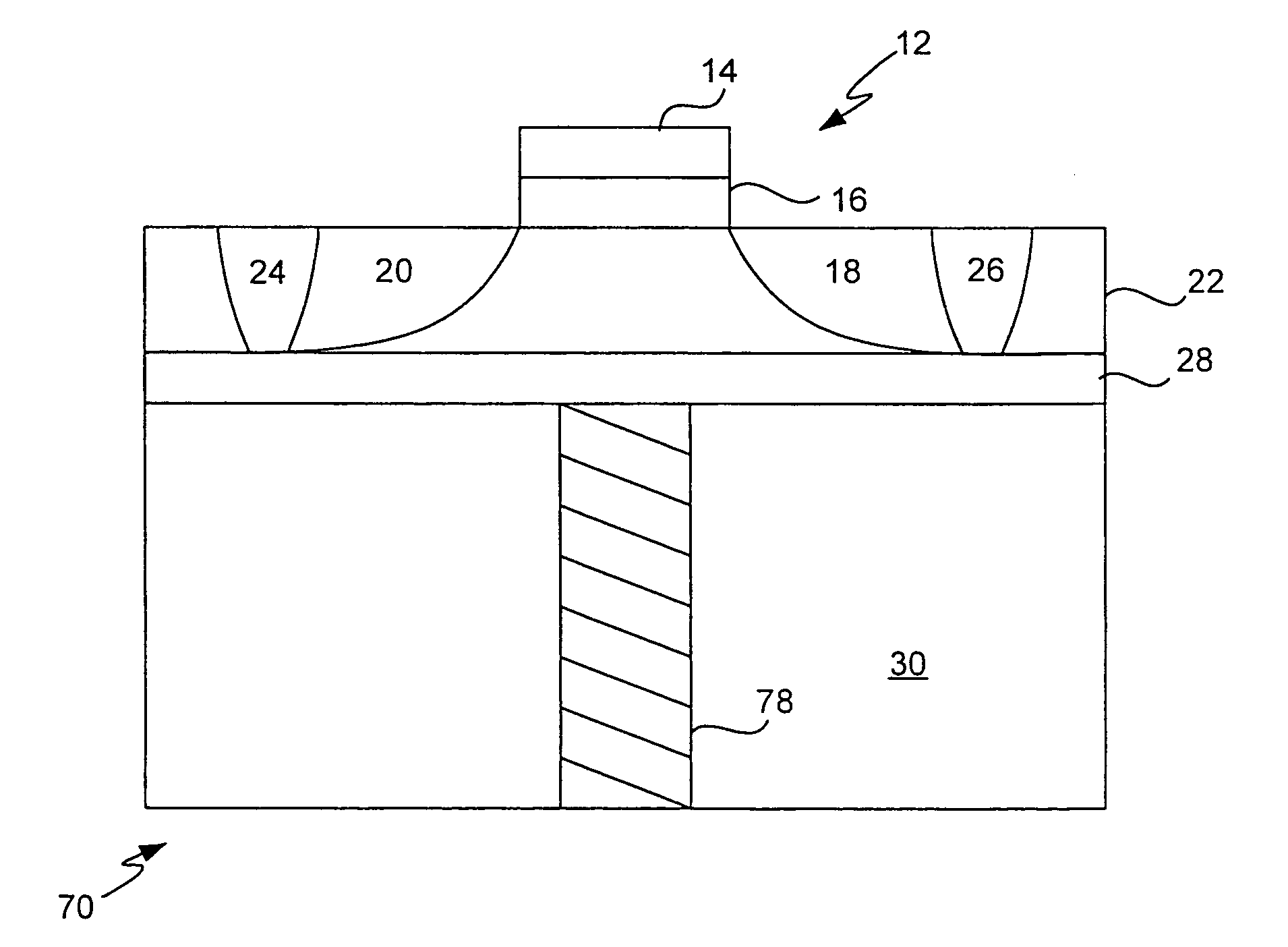
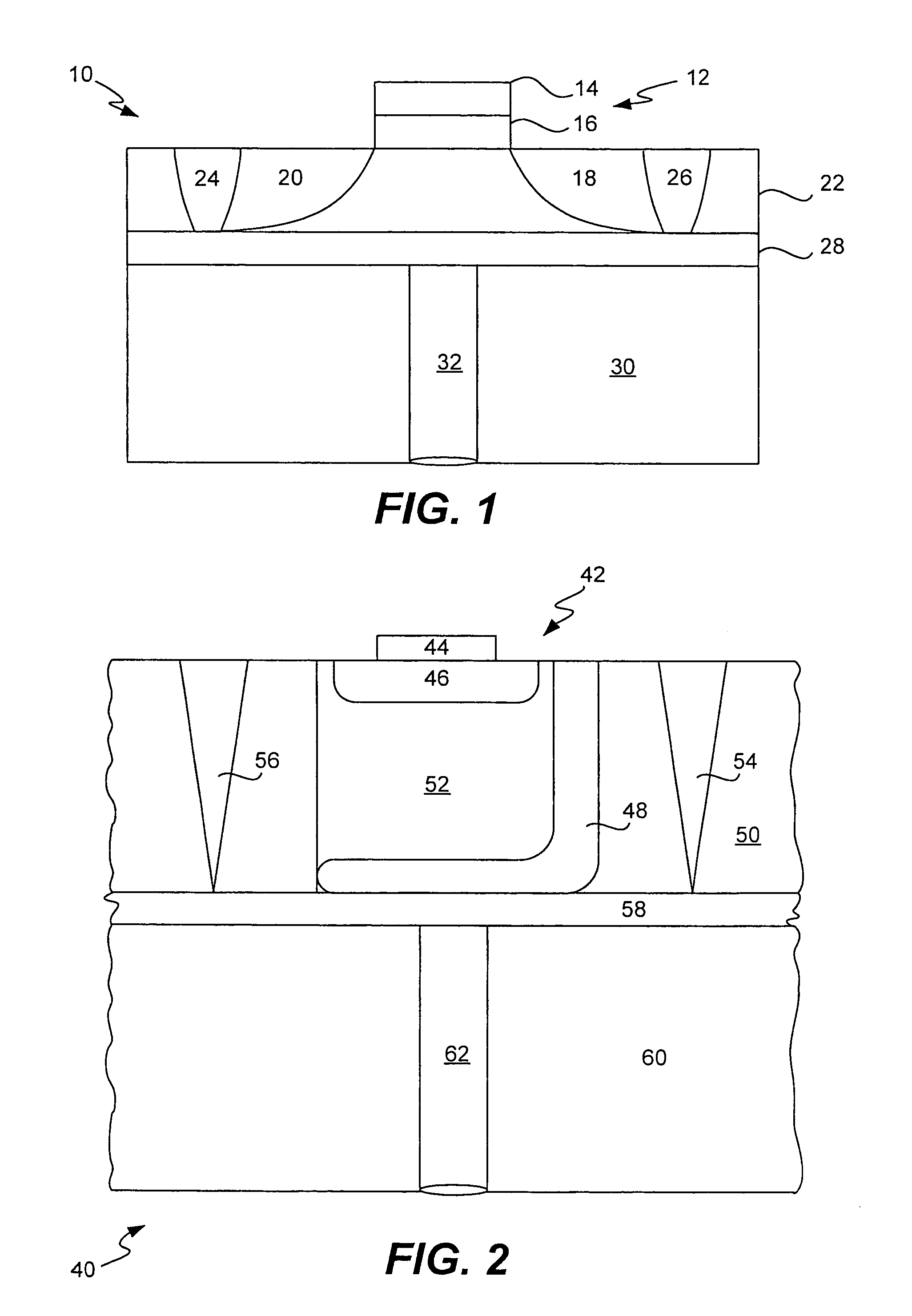
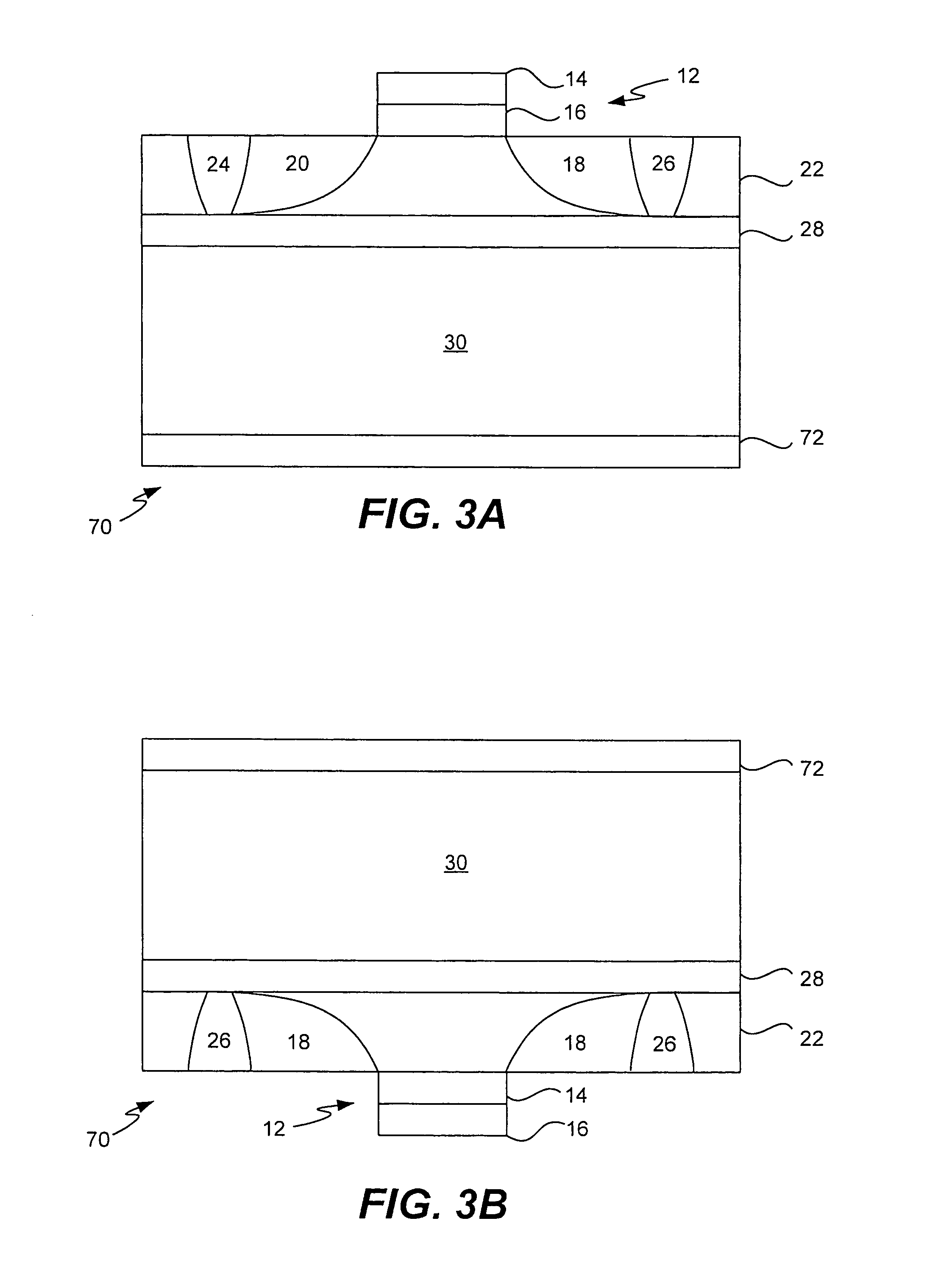
[0014]Referring to FIG. 1, a cross section view of a MOS transistor on a SOI wafer is shown. The wafer 10 includes an MOS transistor 12 having a gate electrode 14, gate oxide 16, and source and drain regions 18 and 20 formed in an active silicon layer 22. Isolation regions 24 and 26, filled with a non-conductive material such as oxide, surround the source and drain regions 18, 20. The active layer 22 is formed over an oxide layer 28 and a bulk silicon layer 30. A heat sink 32, formed in the bulk silicon layer 30, extends from the oxide layer 28 to the bottom surface of the chip 10. In various embodiments of the invention, the heat sink 32 is a plug formed in the bulk silicon layer 30 that is filled with any of a variety of thermally conductive materials, such as copper, aluminum, gold, tungsten, DAG (Thermally conductive paste). In various embodiments of the invention, the heat sink has a circumference ranging from 0.002 mm to 5.0 mm.

[0015]The isolation regions 24 and 26 extend thro...


PUM

PropertyMeasurementUnit
circumferenceaaaaaaaaaa

Abstract

An apparatus and method for a heat sink to dissipate the heat sourced by the encapsulated transistors in a SOI wafer. The apparatus includes a transistor formed in the active silicon layer of the wafer. The active surface is formed over an oxide layer and a bulk silicon layer. A heat sink is formed in the bulk silicon layer and configured to sink heat through the bulk silicon layer, to the back surface of the wafer. After the transistor is fabricated, the heat sink is formed by masking, patterning and etching the back surface of the wafer to form plugs in the bulk silicon layer. The plug extends through the thickness of the bulk layer to the oxide layer. Thereafter, the plug is filled with a thermally conductive material, such as a metal or DAG (thermally conductive paste). During operation, heat from the transistor is dissipated through the heat sink. In various embodiments of the invention, the plug hole is formed using either an anisotropic plasma or wet etch.

Description

FIELD OF THE INVENTION[0001]The present invention relates generally to the fabrication of semiconductor devices, and more particularly, to an apparatus and method for forming heat sinks for silicon on insulator (SOI) type semiconductor wafers.BACKGROUND OF THE INVENTION[0002]For certain high speed and / or high powered integrated circuit applications, silicon on insulator (SOI) chips are desirable. SOI chips are typically fabricated from wafers that have a layer of oxide sandwiched between an active layer of silicon formed on the top surface of the wafer and a bulk layer of silicon formed on the bottom surface of the wafer. Transistors, electrical components, interconnect, and the like, are formed either within or on the active surface of the wafer. The bulk layer is provided to add mechanical strength or rigidity to the wafer.[0003]SOI wafers can be formed using a number of well known techniques. According to one technique, a layer of oxide is grown over the surface of the bulk silic...

Claims


Application Information

Patent Timeline
Patent Type & Authority Patents(United States)
IPC IPC(8): H01L23/34H01L27/12
CPCH01L23/3677H01L29/78606H01L23/481H01L2924/0002H01L2924/00
Inventor HOPPER, PETER J.MIRGORODSKI, IOURIVASHCHENKO, VLADISLAVJOHNSON, PETER
Owner NAT SEMICON CORP
Why Eureka
Try Eureka