Process of manufacturing a piezoelectric element

Inactive Publication Date: 2006-10-17
CANON KK +1
View PDF16 Cites 39 Cited by
  • Summary
  • Abstract
  • Description
  • Claims
  • Application Information

AI Technical Summary

Benefits of technology

[0032]In accordance with the present invention, it is possible to form mono-orientational crystal or monocrystal PZT. Then, as compared with the conventional example, the piezoelectric film can be formed thin with a large piezoelectric constant. As a result, a microprocessing is made applicable to the piezoelectric film, thus providing an elongated liquid discharge recording head having liquid discharge ports formed in high de

Problems solved by technology

Therefore, it is difficult to form the piezoelectric film in a thickness of less than 10 μm, for example.
Thus, the piezoelectric film cannot be processed easily, and makes it difficult to miniaturize the piezoelectric element.
Also, the piezoelectric film formed by burning such powder is subjected to being affected by the crystallized granular boundaries which cannot be ignored when the thickness of film is made smaller to make it impossible to obtain excellent piezoelectric characteristics.
As a result, there is encountered a problem that the piezoelectric film formed by burning the powder cannot provide sufficient piezoelectric characteristics for discharging recording liquid when it is made thinner than 10 μm.
Due to this incapability, it is impossible to materialize a small recording head with the necessary characteristics to discharge recording liquid satisfactorily.
Furthermore, in order to obtain ceramics in high density the dimensional changes due to shrinkage cannot be ignored for the powdered sheet when burning it on the vibration plate, and the structural member of ceramics simultaneously at a temperature of as high as 1,000° C. There is automatically a limit as far as the size is concerned.
It is made difficult, th

Method used


Image

  • Process of manufacturing a piezoelectric element
  • Process of manufacturing a piezoelectric element
  • Process of manufacturing a piezoelectric element

Examples


Example

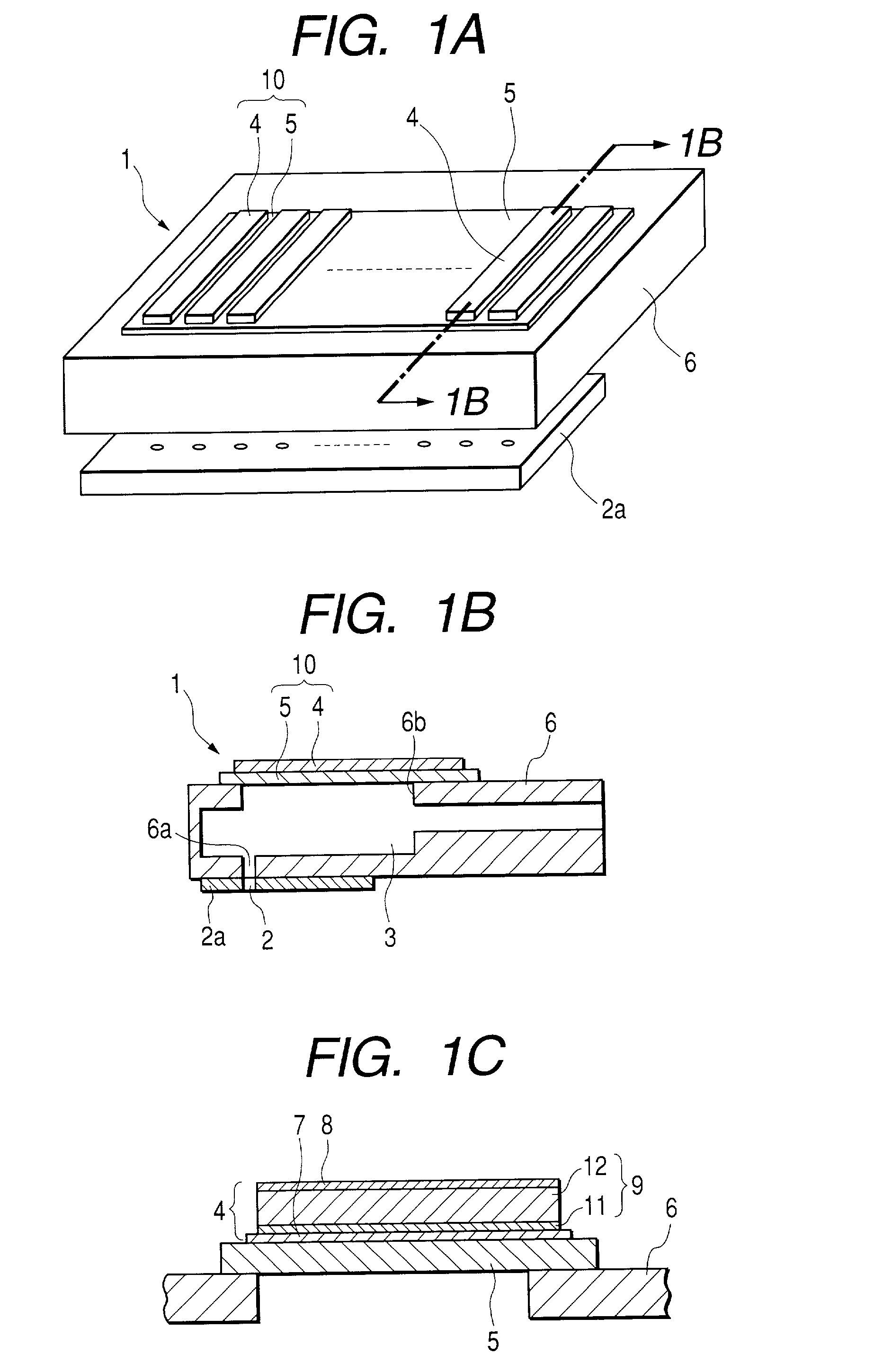
[0043]Hereinafter, in conjunction with the accompanying drawings, the embodiments will be described in accordance with the present invention.

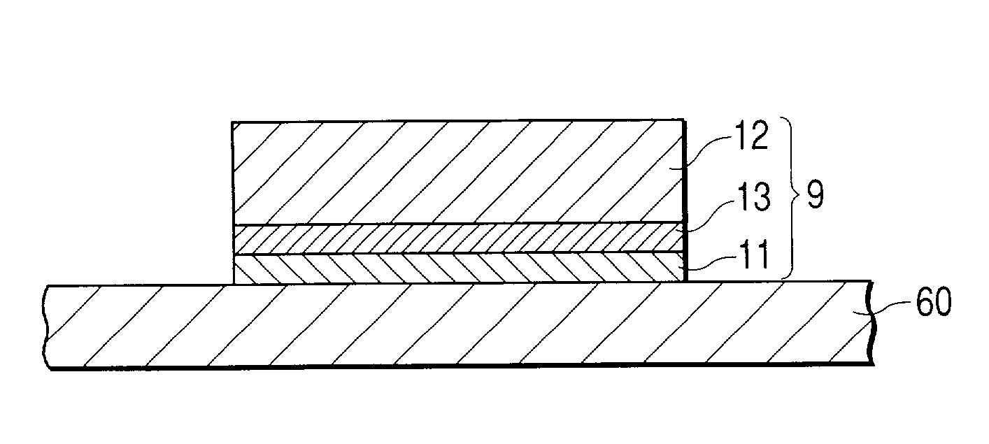
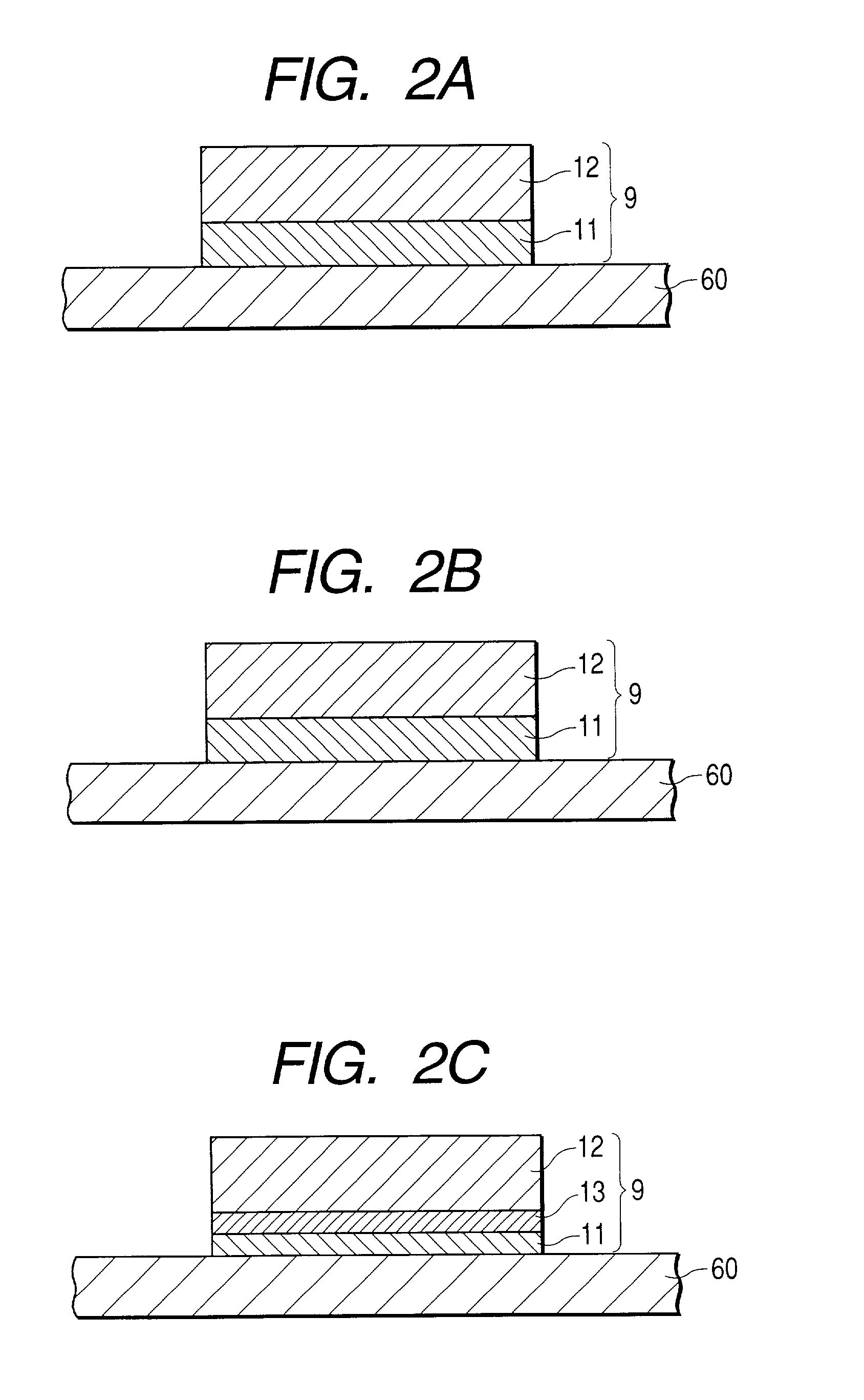
[0044]Of FIGS. 1A to 1C, FIG. 1A is a perspective view which shows a liquid discharge head in accordance with the present invention. FIG. 1B is a cross-sectional view taken along line 1B—1B in FIG. 1A. FIG. 1C is a partially sectional view which shows the piezoelectric vibrating portion in enlargement for the liquid discharge recording head of the invention.

[0045]For the liquid discharge recording head of the present invention, a film formation is executed at a temperature of as high as 500° C. or more using the so-called thin film orientational formation method, such as the sputtering which is regarded as a difficult method to be executed for the purpose conventionally. Then, this head is structured by use of a thin piezoelectric film of monocrystal or mono-orientational crystal having a large piezoelectric constant, which is formed by quick c...


PUM

PropertyMeasurementUnit
Temperatureaaaaaaaaaa
Thicknessaaaaaaaaaa

Abstract

A method of manufacturing a piezoelectric element structure having a supporting substrate and a piezoelectric film supported on the supporting substrate. A first layer, and a second layer having zirconium, each provided with a perovskite structure, are formed in that order on the supporting substrate. The two layers are formed to be in contact with each other or laminated through an intermediate layer. The temperature is set to 500° C. or more at the time of formation of the layers, and cooling is subsequently provided from the formation temperature at least to 450° C. with a cooling speed of 30° C./min or more.

Description

BACKGROUND OF THE INVENTION[0001]1. Field of the Invention[0002]The present invention relates to the liquid discharge recording head which is used for an ink jet recording apparatus, and the method of manufacture therefor. The invention also relates to the structure of piezoelectric element which is used for the liquid discharge recording head or the like.[0003]2. Related Background Art[0004]In recent years, there has been widely used the printer that adopts an ink jet recording apparatus as a printing device for a personal computer or the like, because of the good printing capability, as well as the easier handling and lower costs thereof, among some other advantages. The ink jet recording apparatus has various types, such as to generate bubbles in ink or some other recording liquid by the application of thermal energy, and discharge liquid droplets by means of pressure waves exerted by such bubbling; to suck and discharge liquid droplets by means of electrostatic power; or to disc...

Claims


Application Information

Patent Timeline
IPC IPC(8): H04R17/00B05D5/12B41J2/045B41J2/055B41J2/135B41J2/14B41J2/145B41J2/16C04B35/49C04B35/491C23C14/06H01L41/08H01L41/09H01L41/18H01L41/22H01L41/316H01L41/332H01L41/39
CPCB41J2/161B41J2/1623B41J2/1628B41J2/1629B41J2/1642H01L41/1876H01L41/316B41J2/1646Y10T29/49155B41J2002/14258Y10T29/42H10N30/1051H10N30/8554H10N30/076
Inventor WASA, KIYOTAKAUNNO, AKIRAFUKUI, TETSUROMATSUDA, TAKANORI
Owner CANON KK
Why Eureka
Try Eureka