Method to improve yield and simplify operation of polymer memory cells

a polymer memory cell and polymer technology, applied in the field of improving the yield and functionality of memory cells, can solve the problems of volatile memory devices generally losing their information, the volume, use and complexity of computers and electronic devices are continually increasing, and the initialization process can be shortened. the effect of reducing the need for initialization procedures, reducing the number of initialization procedures, and increasing mobility and availability

Inactive Publication Date: 2006-10-17
CYPRESS SEMICON CORP
View PDF2 Cites 88 Cited by
  • Summary
  • Abstract
  • Description
  • Claims
  • Application Information

AI Technical Summary

Benefits of technology

[0007]The present invention provides for systems and methods of simplifying a polymer memory cell's operation by employing a post polymer growth treatment to form ionic or super ionic metal compounds therein. Such post polymer growth treatment facilitates the distribution and mobility of metal ions (or charged metallic molecules) within an active layer of the polymer memory cell, and mitigates (or eliminates) a need for initialization procedures. Typically, initialization procedures can affect threshold values, and subsequent programming of a polymer memory cells. The thresholds can for example designate a lower limit associated with a particular programming state for the polymer memory cell. Moreover, the present invention can facilitate controlling a distribution of various thresholds (e.g., write and erase threshold), and set them to predetermined values. Accordingly, variability in threshold values of polymer memory cells that typically results from initialization processes can be mitigated or eliminated.
[0009]According to one aspect of the present invention a passive (or superionic) layer(s) (e.g. Cu2S) can be initially formed over a conductive substrate (e.g. copper layer). Over such passive layer, an active polymer layer can be subsequently grown, for example via a CVD process. During such growth a quantity of material from the conductive substrate can become incorporated into the active layer, for example in the form of metal ions or molecular groups (e.g. 2–12% copper concentrations) being trapped or chemically active in the active layer. Next, the active / passive layering arrangement, which can form layering for an organic memory cell, is brought in to contact with post treatment compounds, e.g. (NH4)2S, (NH4)2Se, H2S, H2Se, and H2Te. Such post treatment of the active layer increases a mobility and availability of the metal ions incorporated therein, and mitigates a need for initialization procedures; e.g. by subjecting the active / passive layers to an initial electric field to provide a supply of positive ions within the polymer active layer. As such, performance variations in a polymer memory cell that can result from the initialization process can be reduced, allowing thicker polymer films to be efficiently employed as part of the active layer. Typically, such can also increase the polymer memory cell yield.
[0010]In a related aspect of the present invention, the polymer memory cell treated with the post treatment compounds can be programmed by being subjected to an external stimulus. Such an external stimulus can be supplied via a control component, and can influence an electrical or optical property associated with the polymer memory cell. The control component can further control the external stimulus, and thereby regulate and / or trace the influenced property of the organic memory cell. Such programming can typically provide for stability, viability and fast switching of a memory cell's operation at a single or multi-bit level.
[0011]According to yet another aspect of the present invention, exposure of active and passive layers to the post treatment compounds (e.g., (NH4)2S, (NH4)2Se, H2S, H2Se, and H2Te) can be regulated via a controlled process depending on various factors, such as for example: thickness of the active polymer layer, composition of the polymer layer, concentration of positive ions in the polymer, and the like. Such exposure can also densify the polymer, and reduce void formation in underlying copper metallization, when copper plugs are employed as part of the polymer memory cell.

Problems solved by technology

The volume, use and complexity of computers and electronic devices are continually increasing.
The long term storage mediums typically store larger amounts of information at a lower cost, but are slower than other types of storage devices.
Volatile memory devices generally lose their information if they lose power and typically require periodic refresh cycles to maintain their information.
However, silicon-based devices are approaching their fundamental physical size limits.
Inorganic solid state devices are generally encumbered with a complex architecture which leads to high cost and a loss of data storage density.
The volatile semiconductor memories based on inorganic semiconductor material must constantly be supplied with electric current with a resulting heating and high electric power consumption in order to maintain stored information.
In addition, employment of organic materials typically can require cumbersome initialization procedures that can adversely affect performance of such devices.

Method used


Image

  • Method to improve yield and simplify operation of polymer memory cells
  • Method to improve yield and simplify operation of polymer memory cells
  • Method to improve yield and simplify operation of polymer memory cells

Examples


Embodiment Construction

[0024]The present invention is now described with reference to the drawings, wherein like reference numerals are used to refer to like elements throughout. In the following description, for purposes of explanation, numerous specific details are set forth in order to provide a thorough understanding of the present invention. It may be evident, however, that the present invention may be practiced without these specific details. In other instances, well-known structures and devices are shown in block diagram form in order to facilitate describing the present invention.

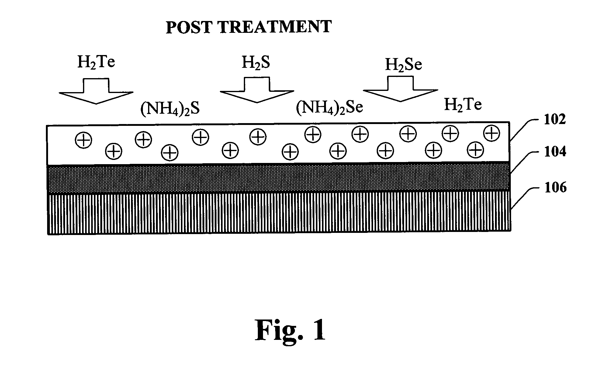
[0025]The present invention provides for a post polymer growth treatment with compounds that can react with the active layer's metallic clusters to create metal ions (or charged metallic molecules) therein. Such compounds can for example include: ammonium sulfate (NH4)2S, ammonium selenide (NH4)2Se, hydrogen sulfide (H2S), hydrogen selenide (H2Se), hydrogen telluride (H2Te) and the like. The post treatment methodology of ...


PUM


Abstract

Systems and methodologies are provided for simplifying a polymer memory cell's operation by employing a post polymer growth treatment to form ionic or super ionic metal compounds therein. Such post polymer growth treatment facilitates distribution and mobility of metal ions (or charged metallic molecules) within an active layer of the polymer memory cell, and mitigates (or eliminates) a need for initialization procedures. Moreover, the post treatment of the present invention can also facilitate controlling a distribution of various thresholds (e.g., write and erase threshold), and set them to predetermined values Accordingly, variability in threshold values of polymer memory cells that can result from initialization processes can be mitigated (or eliminated), and thicker polymer layers can be employed without an initialization penalty.

Description

TECHNICAL FIELD[0001]The present invention relates generally to improving yield and functionality of memory cells, and in particular to post treatment and exposure of polymer memory cell layers to compounds that can react with metal particles therein to create metal ions (or charged metallic molecules), thus mitigating a need for an initialization of the polymer memory cell.BACKGROUND OF THE INVENTION[0002]The volume, use and complexity of computers and electronic devices are continually increasing. Computers consistently become more powerful, new and improved electronic devices are continually developed (e.g., digital audio players, video players). Additionally, the growth and use of digital media (e.g., digital audio, video, images, and the like) have further pushed development of these devices. Such growth and development has vastly increased the amount of information desired / required to be stored and maintained for computer and electronic devices.[0003]Generally, information is ...

Claims


Application Information

Patent Timeline
Patent Type & Authority Patents(United States)
IPC IPC(8): H01L35/24H01L51/00
CPCG11C13/0014G11C13/0016H10K19/202
Inventor GAUN, DAVIDSPITZER, STUARTYUDANOV, NICOLAY F
Owner CYPRESS SEMICON CORP
Why Eureka
Try Eureka