Wired circuit board

a wired circuit board and wire technology, applied in the field of wired circuit boards, can solve the problems of increasing noise on the signal, increasing the requirement of flexible wired circuit boards with metal substrates, and increasing the influence of noise on signals, so as to improve the reliability of electrical connections, reduce noise, and ensure the effect of connection reliability

Active Publication Date: 2006-11-07
NITTO DENKO CORP
View PDF7 Cites 54 Cited by
  • Summary
  • Abstract
  • Description
  • Claims
  • Application Information

AI Technical Summary

Benefits of technology

[0013]It is the object of the present invention to provide a wired circuit board that can provide enhanced reliability of electrical connection between a metal substrate and a shield layer to achieve significant noise reduction reliably.
[0015]According to the present invention, the shield layer covering the insulating cover layer and connected to the metal substrate is closely contacted with the resin layers at its end portions on the opposite side of the insulating cover layer to the connecting portion of the shield layer with the metal substrate. This can produce the advantageous result that even when the shield layer is formed by plating or by a vacuum film-forming method, the shield layer can be closely contacted with the resin layers at end portions thereof in a reliable manner. This can prevent the shield layer from stripping from the end portions thereof so as to ensure a reliable connection of the shield layer with the metal substrate at the connecting portion thereof. This can provide enhanced reliability of electrical connection between the metal substrate and the shield layer to achieve significant noise reduction reliably.

Problems solved by technology

Along with an increasing demand for size reduction and high integration of an electric device or an electronic device in recent years, required qualities for a flexible wired circuit board with a metal substrate, such as, for example, finer pattern of the wired circuit and higher thickness precision constituent material, are increasingly becoming severe.
The finer the wired circuit pattern becomes, the higher and weaker the signal frequency becomes particularly in a suspension board with circuit to be mounted on a hard disk drive, so that influence of noise on the signal is increasingly becoming noticeable.
However, these proposals are not sufficient for the noise reduction required in these days.
However, JP Unexamined Patent Publication No. 2003-69170 cited above has the disadvantage that since the conductor layer is formed by a conductive tape or film, the conductor layer strips off too easily.

Method used


Image

  • Wired circuit board
  • Wired circuit board
  • Wired circuit board

Examples


example 1

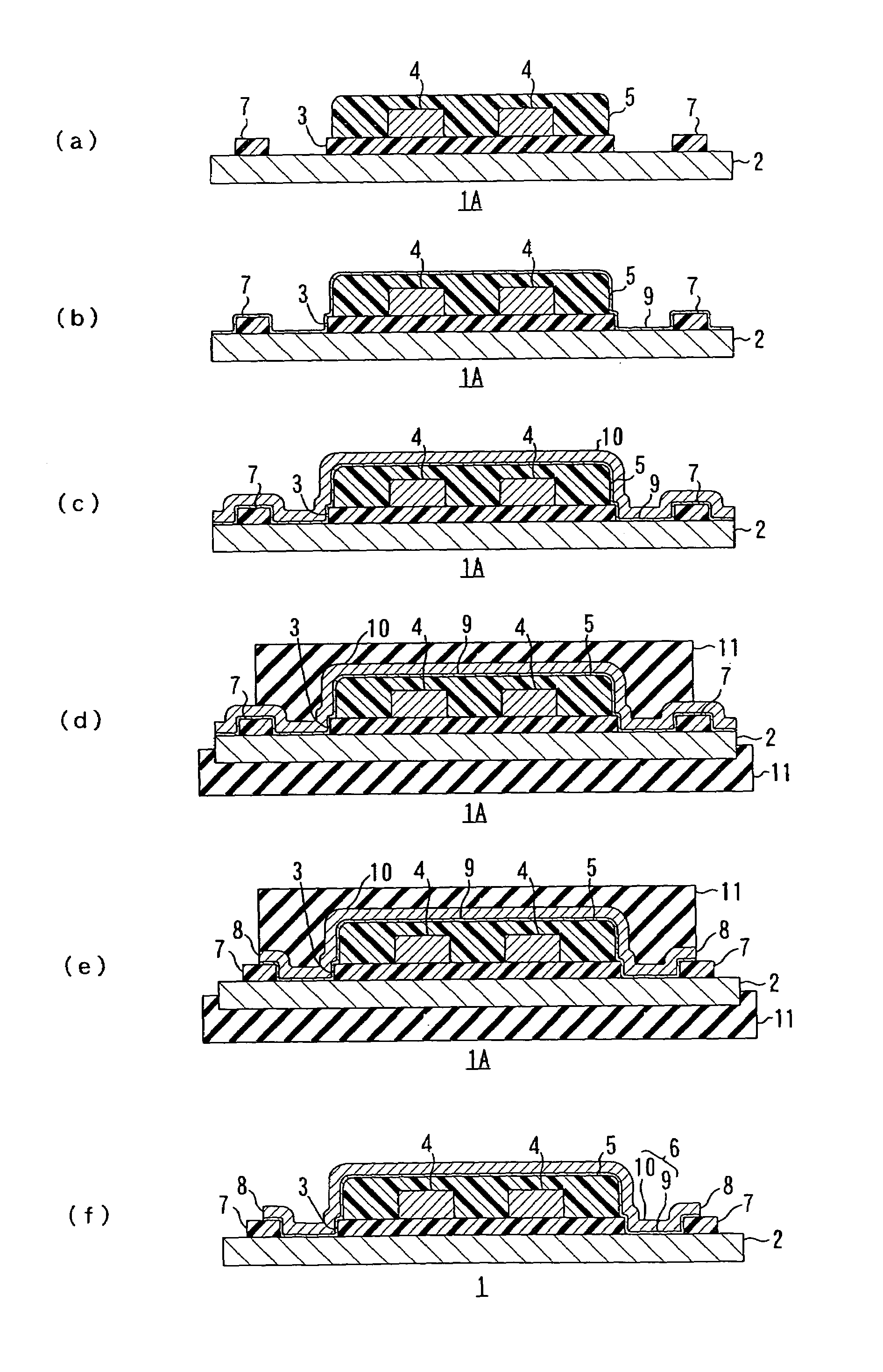
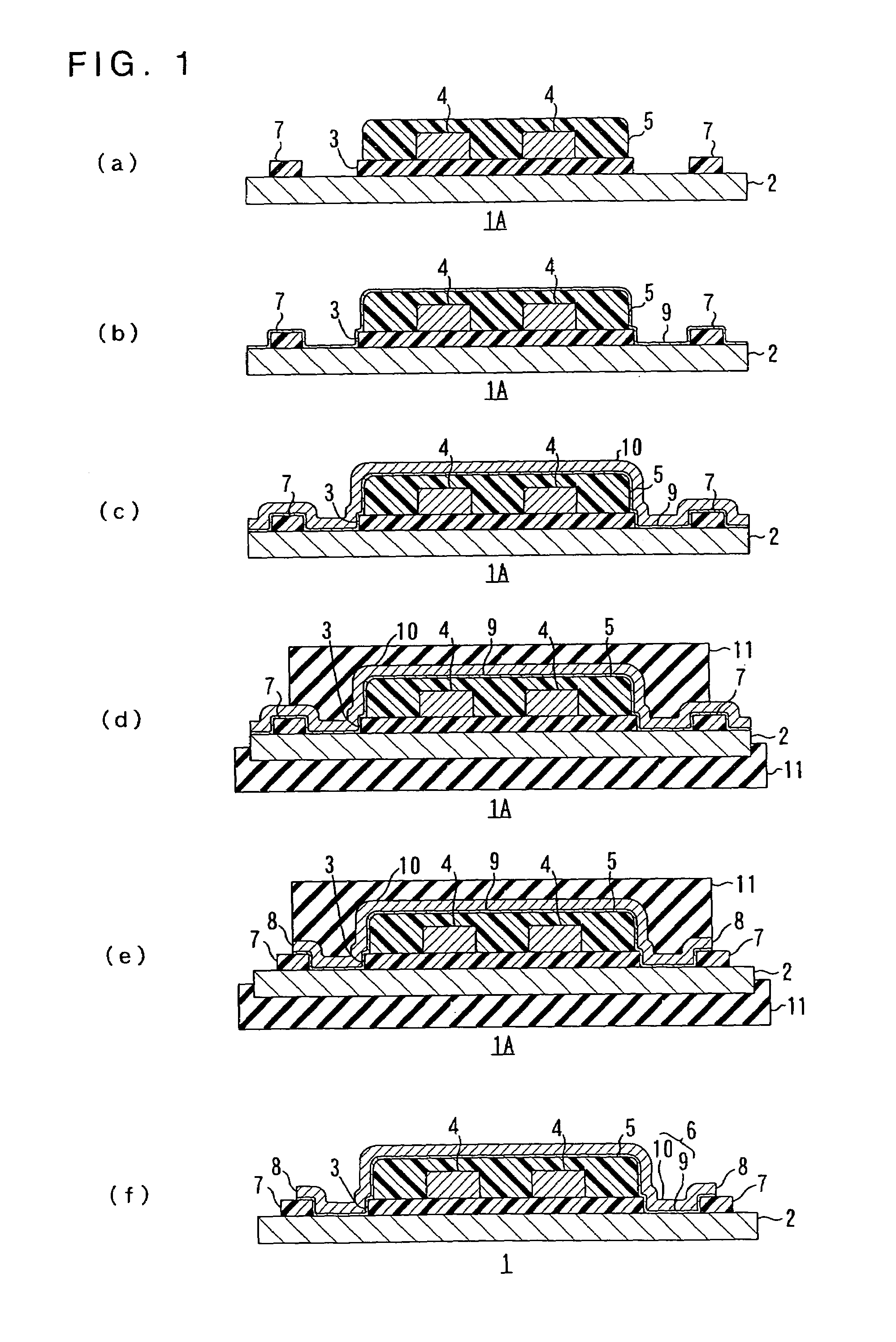
[0105]Solution of polyamic acid resin was applied to a surface of a metal substrate of stainless foil having thickness of 20 μm and then was exposed to light and developed. Thereafter, it is cured, whereby an insulating base layer of polyimide resin having thickness of 14 μm and two resin layers of polyimide resin having thickness of 14 μm and width of 0.1 mm and spaced 0.1 mm from both widthwise sides of the insulating base layer were formed in the form of a predetermined pattern.

[0106]Then, a conductor layer was formed by a semi-additive process. Specifically, a thin metal film comprising a thin chromium film having thickness of 300 Å and a thin copper film having thickness of 700 Å were formed by sputtering. Then, an electrolytic copper-plated layer having thickness of 10 μm was formed on the thin metal film thus formed. Then, the electrolytic copper-plated layer was covered with an electroless nickel-plated layer having thickness of 0.1 μm by electroless nickel plating.

[0107]The...

example 2

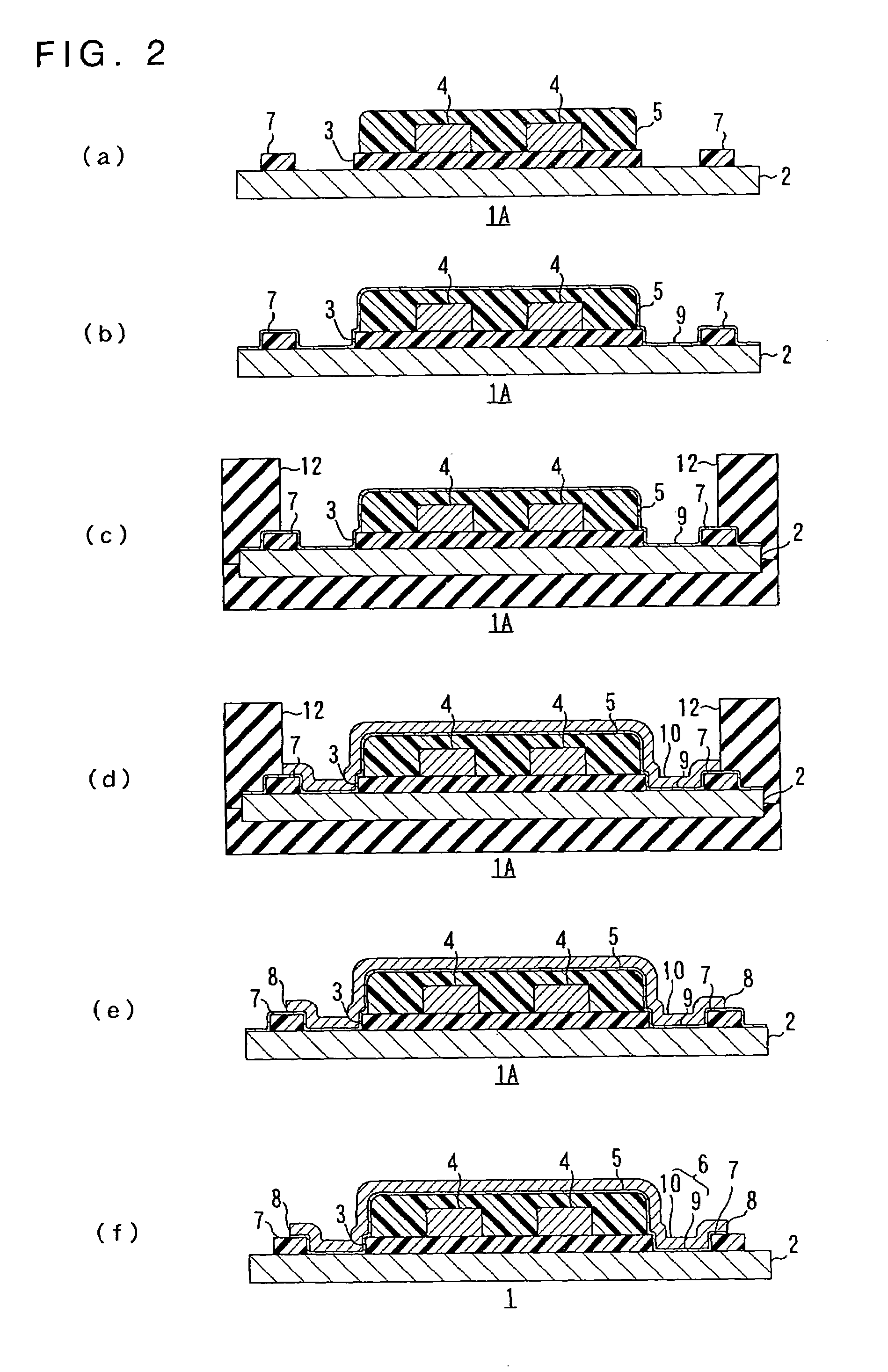
[0111]The wired circuit board before the shield layer being formed was produced in the same manner as in Example 1 (Cf. FIG. 2(a)).

[0112]Then, a thin metal film comprising a thin chromium film having thickness of 300 Å and a thin copper film having thickness of 700 Å was formed on the entire area of the metal substrate including the insulating cover layer and the resin layers by sputtering (Cf. FIG. 2(b)).

[0113]Thereafter, a plating resist of dry film resist was formed on a portion of the thin conductor film corresponding to a reversed portion of the shield layer forming portion (Cf. FIG. 2(c)). Then, an electrolytic plated layer comprising an electrolytic nickel-plated layer having thickness of 1 μm and an electrolytic gold-plated layer having thickness of 1 μm was formed by electrolytic nickel plating and electrolytic gold plating on the thin conductor film exposed from the plating resist (Cf. FIG. 2(d)). Thereafter, the plating resist was removed by chemical etching (Cf. FIG. 2(e...

example 3

[0114]The wired circuit board before the shield layer being formed was produced in the same manner as in Example 1 (Cf. FIG. 3(a)).

[0115]Then, a thin metal film comprising a thin chromium film having thickness of 300 Å and a thin copper film having thickness of 700 Å was formed on the entire area of the metal substrate including the insulating cover layer and the resin layers by sputtering (Cf. FIG. 3(b)).

[0116]Then, an etching resist of dry film resist was formed on a shield layer forming portion of the thin conductor film (FIG. FIG. 3(c)). Then, the thin conductor film exposed from the etching resist was removed by chemical etching (Cf. FIG. 3(d)).

[0117]Thereafter, the etching resist was removed by chemical etching (FIG. 4(e)). Then, a plating resist of dry film resist was formed on a portion of the metal substrate corresponding to a reversed portion of the shield layer forming portion thereof (FIG. 4(f)).

[0118]Then, an electrolytic plated layer comprising an electrolytic nickel-p...


PUM


Abstract

A wired circuit board is provided having enhanced reliability of electrical connection between a metal substrate and a shield layer to achieve significant noise reduction reliably. An insulating base layer is formed on the metal substrate, while resin layers are formed on the metal substrate with a predetermined space provided from the both widthwise sides of the insulating base layer. A conductor layer is formed having a predetermined wired circuit pattern on the insulating base layer. Thereafter, an insulating cover layer is formed on the insulating base layer in such a manner as to cover the conductor layer. Then, a shield layer is laminated on the metal substrate to cover the insulating cover layer and also is put in close contact with the resin layers at end portions thereof by a vacuum film-forming method or by plating.

Description

[0001]This application claims priority from Japanese Patent Application No. 2003-159134, filed Jun. 4, 2003, the entire contents of which are herein incorporated by reference to the extent allowed by law.BACKGROUND OF THE INVENTION[0002]1. Field of the Invention[0003]The present invention relates to a wired circuit board and, more particularly, to a flexible wired circuit board with a metal substrate having a shield layer formed thereon.[0004]2. Description of the Prior Art[0005]Along with an increasing demand for size reduction and high integration of an electric device or an electronic device in recent years, required qualities for a flexible wired circuit board with a metal substrate, such as, for example, finer pattern of the wired circuit and higher thickness precision constituent material, are increasingly becoming severe.[0006]The finer the wired circuit pattern becomes, the higher and weaker the signal frequency becomes particularly in a suspension board with circuit to be m...

Claims


Application Information

Patent Timeline
Patent Type & Authority Patents(United States)
IPC IPC(8): H05K1/03H05K1/05H05K1/02H05K3/46
CPCH05K1/0218H05K1/056H05K3/4644H05K2201/09554
Inventor YOSHIMI, TAKESHIOSAWA, TETSUYA
Owner NITTO DENKO CORP
Why Eureka
Try Eureka