System and method for using dynamic random access memory and flash memory

a dynamic random access and flash memory technology, applied in the field of computer memory systems, can solve the problems of inability to achieve higher capacity, read time impair the compatibility of srams, etc., and achieve the effect of high storage capacity and high speed

Inactive Publication Date: 2006-11-14
HITACHI ULSI SYST CO LTD +1
View PDF19 Cites 113 Cited by
  • Summary
  • Abstract
  • Description
  • Claims
  • Application Information

AI Technical Summary

Benefits of technology

[0012]An object of the present invention is to provide a memory system including ROM and RAM, wh

Problems solved by technology

This poses a problem in that needs for higher capacity cannot be achiev

Method used


Image

  • System and method for using dynamic random access memory and flash memory
  • System and method for using dynamic random access memory and flash memory
  • System and method for using dynamic random access memory and flash memory

Examples


first embodiment

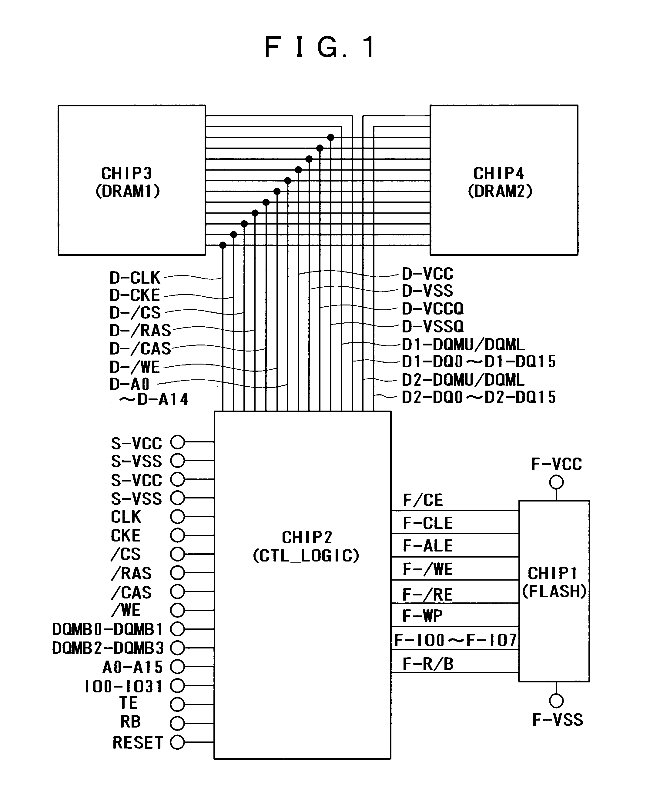
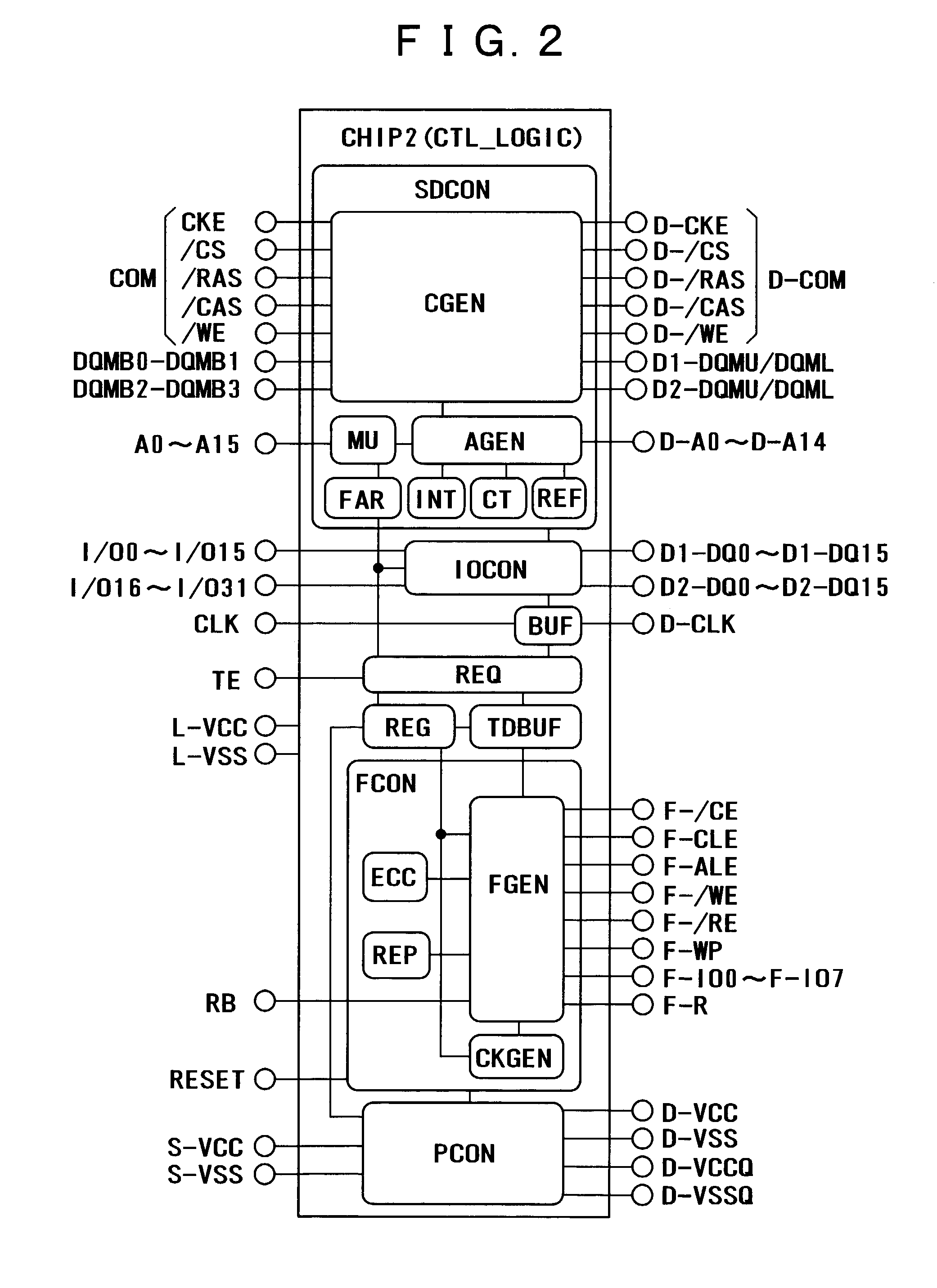
[0054]FIG. 1 illustrates a memory module which is an example of the application of the memory system related to the present invention. The memory module consists of four chips. Each of the chips will be described below.

[0055]First, CHIP1 (flash memory, hereafter referred to as “FLASH”) is a nonvolatile memory. For the nonvolatile memory, ROM (Read-Only Memory), EEPROM (Electrically Erasable and Programmable ROM), flash memory, or the like can be used. Flash memory will be taken as an example for the embodiment. CHIP2 (CTL_LOGIC) includes a control circuit which controls CHIP1, CHIP3, and CHIP4. CHIP3 and CHIP4 are dynamic random access memories (DRAMs). There are various types of DRAM, including EDO (Extended Data Out), SDRAM (Synchronous DRAM), and DDR (Double Data Rate), depending on differences in internal constitution and interface. Any DRAM is applicable to the memory module but SDRAM will be taken as an example for the description of the embodiment.

[0056]To the memory module, ...

second embodiment

[0258]FIGS. 27A and 27B illustrate a memory module to which the memory system of the present invention is applied. FIG. 27A is a top view of the memory module and FIG. 27B is a cross-sectional view taken along the line A–A′ of the top view.

[0259]In the memory module in this embodiment, CHIP1 (FLASH), CHIP2 (CTL_LOGIC), CHIP3 (DRAM1) and CHIP4 (DRAM2) are mounted on a board PCB (for example, printed circuit board composed of a glass-epoxy substrate) which board is to be mounted on a device through ball grid array (BGA). A bare chip of general purpose DRAM wherein signal and power supply pads are arranged in line in the center of the so-called chip is used for CHIP3 and CHIP4, without confinement thereto. A general purpose bare chip of FLASH wherein signal and power supply pads are arrange in line at one end of the so-called chip is used for CHIP1, without confinement thereto.

[0260]The bonding pads on CHIP1 and the bonding pads on the board PCB are connected with each other through bo...


PUM


Abstract

A system and method are provided for using dynamic random access memory and flash memory. In one example, the memory system comprises a nonvolatile memory; synchronous dynamic random access memories; circuits including a control circuit which is coupled with the nonvolatile memory and the synchronous dynamic random access memories, and controls accesses to the nonvolatile memory and the synchronous dynamic random access memories; and a plurality of input/output terminals coupled with the circuits, wherein in data transfer from the nonvolatile memory to the synchronous dynamic random access memories, error corrected data is transferred.

Description

COPYRIGHT NOTICE[0001]A portion of the disclosure of this patent document contains material which is subject to copyright protection. The copyright owner has no objection to the facsimile reproduction by anyone of the patent document or the patent disclosure, as it appears in the Patent and Trademark Office patent file or records, but otherwise reserves all copyright rights whatsoever.BACKGROUND OF THE INVENTION[0002]1. Field of the Invention[0003]The present invention generally relates to computer memory systems and, more particularly, to memory systems having dynamic random access memories (DRAMs) and to control methods such memory systems.[0004]2. Discussion of Background[0005]There are conventionally combination semiconductor memories wherein flash memory (capacity: 32 megabits) and static random access memory (SPAM (capacity: 4 megabits)) on a stack chip (stack) are integrally sealed in an FBGA (Fine pitch Ball Grid Array) package. The flash memory and the SRAM use the input / ou...

Claims


Application Information

Patent Timeline
IPC IPC(8): G06F12/00G06F12/02G06F12/16G06F12/06G11C7/00G11C11/34G11C11/401G11C16/02
CPCG06F11/1068G06F12/0638Y02B60/1225Y02D10/00G11C11/34
Inventor MIURA, SEIJIAYUKAWA, KAZUSHIGEIWAMURA, TETSUYA
Owner HITACHI ULSI SYST CO LTD
Why Eureka
Try Eureka