Substrate processing apparatus and method

a processing apparatus and substrate technology, applied in the direction of liquid/solution decomposition chemical coating, semiconductor/solid-state device details, coatings, etc., can solve the problems of poor throughput, copper diffusion fear, interconnection exposed at the bottom of contact holes, etc., to achieve effective removal of hydrogen gas generated during plating and carry out plating stably

Inactive Publication Date: 2006-11-28
EBARA CORP
View PDF4 Cites 16 Cited by
  • Summary
  • Abstract
  • Description
  • Claims
  • Application Information

AI Technical Summary

Benefits of technology

[0026]According to the substrate plating method, a flow of plating solution is stopped during the progress of plating. This can prevent a flow of plating solution from affecting the results of plating. It is possible to allow the substrate

Problems solved by technology

When an additional embedded interconnect structure is formed on such an exposed surface of interconnects of a semiconductor substrate, the following problems may be encountered.
Further, upon etching of the SiO2 layer for the formation of contact holes, the pre-formed interconnects exposed at the bottoms of the contact holes can be contaminated with an etchant, a peel

Method used


Image

  • Substrate processing apparatus and method
  • Substrate processing apparatus and method
  • Substrate processing apparatus and method

Examples


Embodiment Construction

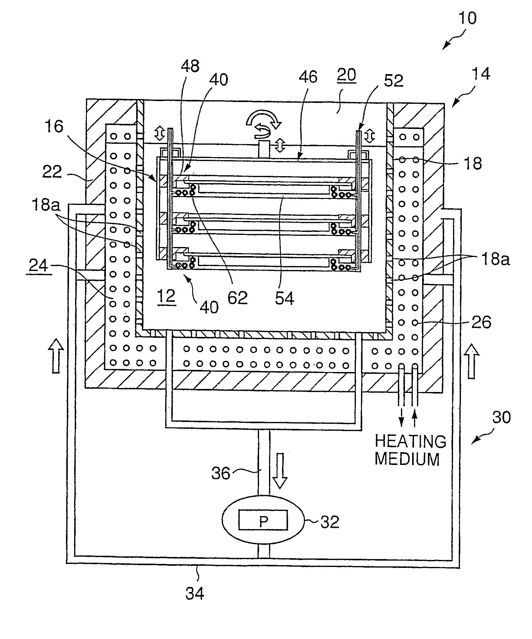
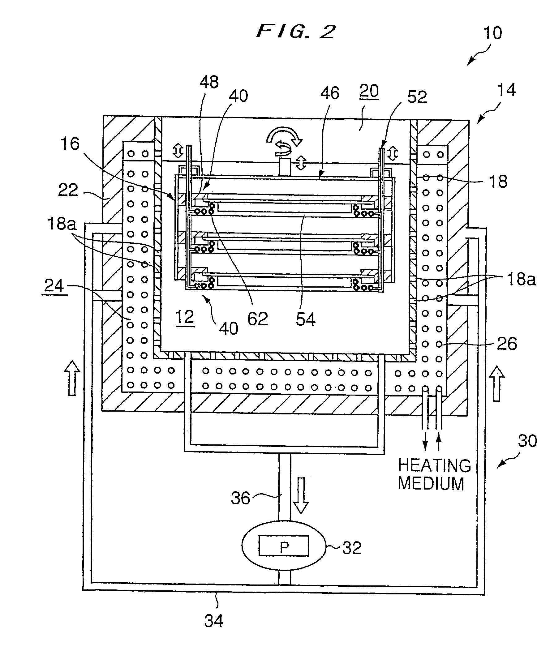
[0051]Preferred embodiments of the present invention will now be described in detail with reference to the accompanying drawings, which in no way limit the invention.

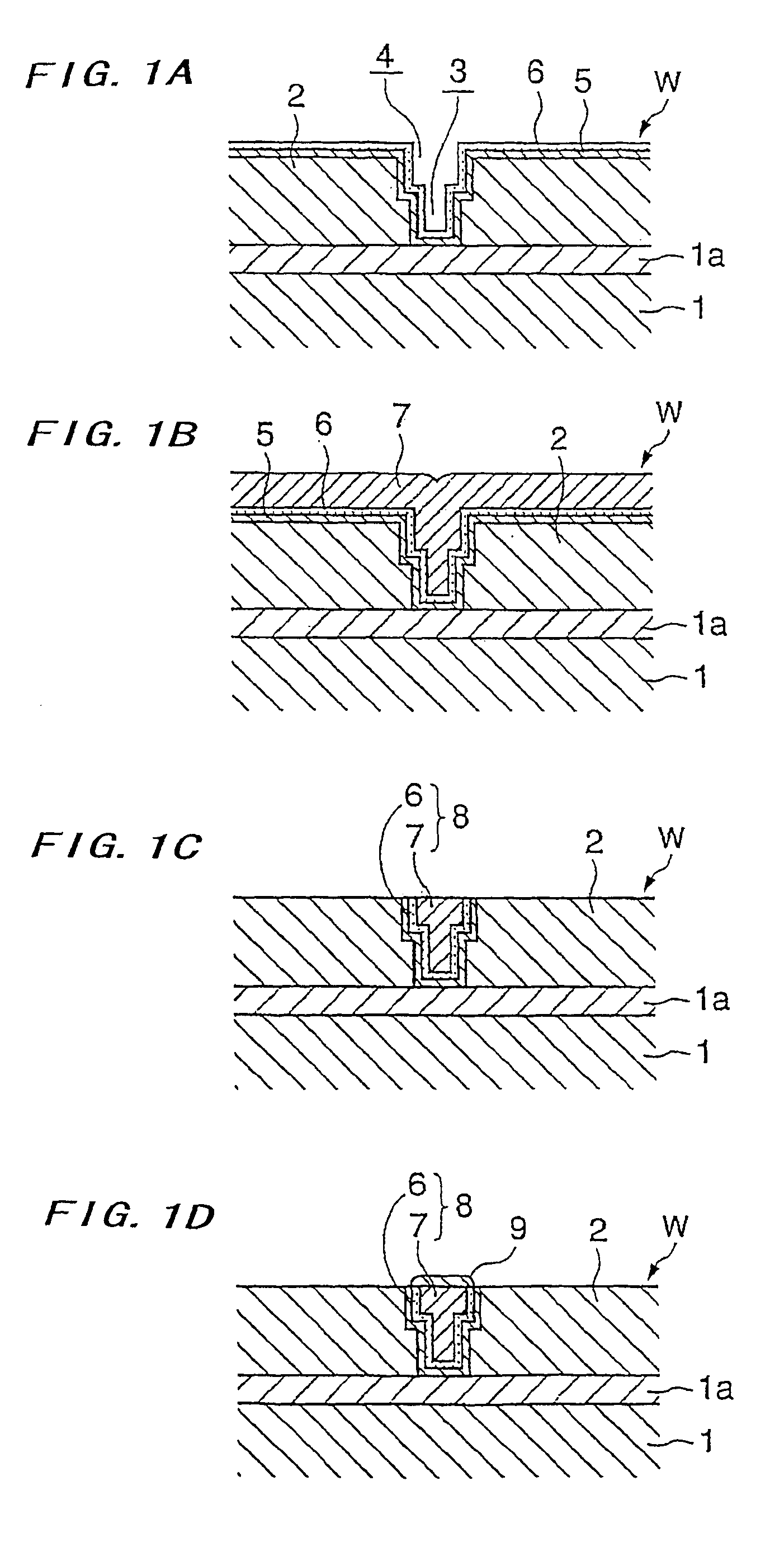
[0052]FIGS. 1A through 1D illustrate, in sequence of process steps, an example of the formation of copper interconnects in a semiconductor device. As shown in FIG. 1A, an insulating film 2 of e.g. SiO2 is deposited on a conductive layer 1a in which semiconductor devices are provided, which is formed on a semiconductor base 1. Contact holes 3 and trenches 4 for interconnects are formed in the insulating film 2 by the lithography / etching technique. Thereafter, a barrier layer 5 of TaN or the like is formed on the entire surface, and a copper seed layer 6 as an electric supply layer for electroplating is formed on the barrier layer 5, for example, by sputtering.

[0053]Thereafter, as shown in FIG. 1B, copper plating is carried out onto the surface of the semiconductor substrate W to fill the contact holes 3 and the trenches ...


PUM

PropertyMeasurementUnit
Temperatureaaaaaaaaaa

Abstract

A substrate processing apparatus and method which employs the so-called batch processing method of processing a plurality of substrates simultaneously, thereby increasing the throughput, and which can carry out processing, such as electroless plating, stably and securely with a relatively simple apparatus. The substrate processing apparatus includes: a processing bath (14) for holding a processing liquid (12); and a substrate holder (16) which is vertically movable relative to the processing bath (14) and which includes a plurality of substrate holding portions (40) for holding a plurality of substrates (W) in parallel. Each substrate holding portion (40) has a substrate stage (48) and a substrate presser (54), which can move close to or away from each other and can grip therebetween a peripheral portion of a substrate to thereby hold the substrate with its back surface sealed, and has a heating medium flow passage (62) for passing a heating medium therethrough so as to regulate the temperature of the substrate holding portion (40).

Description

BACKGROUND OF THE INVENTION[0001]1. Technical Field of the Invention[0002]This invention relates to a substrate processing apparatus and method, more particularly, relates to a substrate processing apparatus and method useful for forming embedded interconnects that an electric conductor, such as copper or silver, is embedded in fine recesses for interconnects formed in the surface of a substrate like a semiconductor substrate, and for forming a protective layer for protecting the surface of the interconnects.[0003]2. Description of the Related Art[0004]An electroless plating is such a method that a plated film is formed on a plating surface of a workpiece by chemically reducing metal ions in a plating solution without supplying any electric current from the outside, and the electroless plating is widely used in a nickel-phosphorus plating and a nickel-boron plating for giving a corrosion resistance and a wear resistance, and a copper plating for a printed-wiring substrate.[0005]As a...

Claims


Application Information

Patent Timeline
IPC IPC(8): B05D1/18C23C18/16C23C18/31H01L21/288H01L21/3205H01L21/768H01L23/52
CPCC23C18/1628H01L21/288H01L21/76843H01L21/76849H01L21/76874H01L21/76864
Inventor WANG, XINMINGABE, KENICHIMISHIMA, KOJI
Owner EBARA CORP
Why Eureka
Try Eureka