Controlled collapse chip connection (C4) integrated circuit package which has two dissimilar underfill materials

a technology of integrated circuits and underfill materials, which is applied in the direction of electrical equipment, semiconductor devices, semiconductor/solid-state device details, etc., can solve the problems of voids in the underfill material, and low production efficiency of ceramic materials

Inactive Publication Date: 2006-11-28
MICRON TECH INC
View PDF59 Cites 14 Cited by
  • Summary
  • Abstract
  • Description
  • Claims
  • Application Information

AI Technical Summary

Problems solved by technology

Air voids weaken the structural integrity of the integrated circuit/substrate interface.
Ceramic materials are relatively expensive to produce in mass quantities.
The release of moisture during the underfill process may create voids in the underfill material.
Organic substrates also tend to have a higher coefficient of thermal expansion compared to ceramic substrat...

Method used


Image

  • Controlled collapse chip connection (C4) integrated circuit package which has two dissimilar underfill materials
  • Controlled collapse chip connection (C4) integrated circuit package which has two dissimilar underfill materials
  • Controlled collapse chip connection (C4) integrated circuit package which has two dissimilar underfill materials

Examples


Embodiment Construction

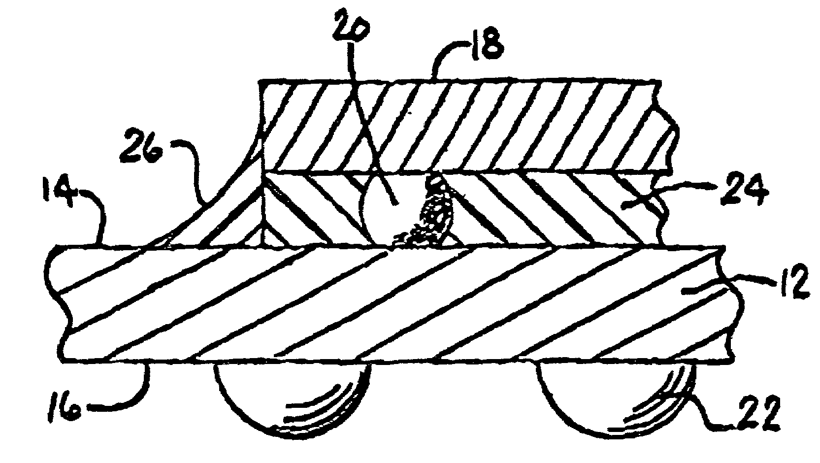
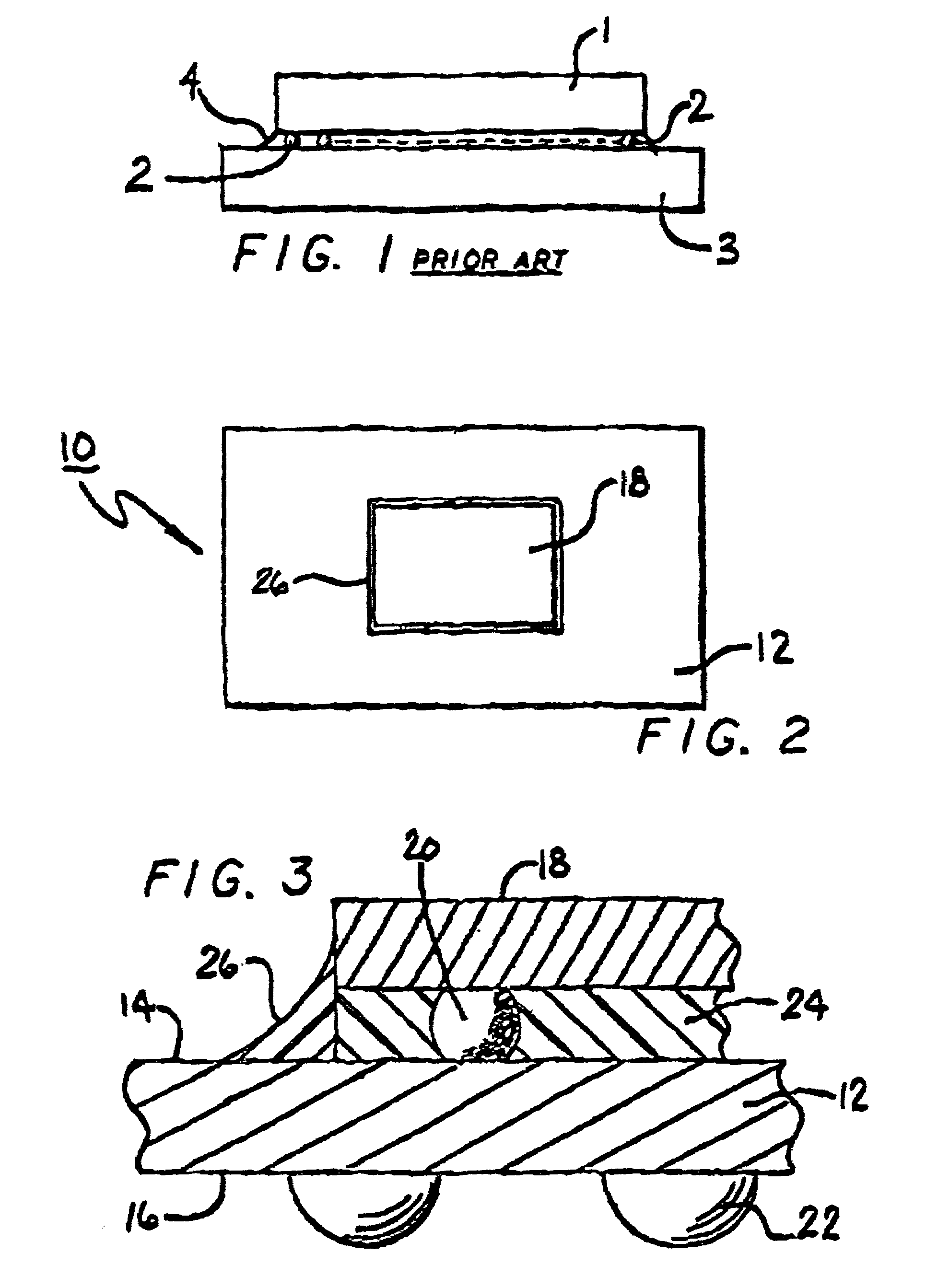
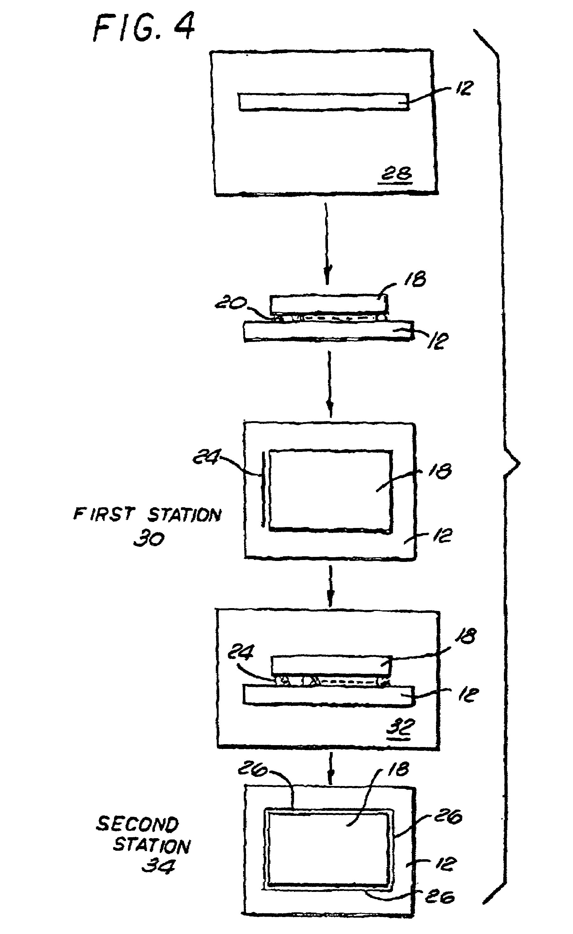
[0016]Referring to the drawings more particularly by reference numbers, FIGS. 2 and 3 show an embodiment of an integrated circuit package 10 of the present invention. The package 10 may include a substrate 12 which has a first surface 14 and a second opposite surface 16. An integrated circuit 18 may be attached to the first surface 14 of the substrate12 by a plurality of solder bumps 20. The solder bumps 20 may be arranged in a two-dimensional array across the integrated circuit 18. The solder bumps 20 may be attached to the integrated circuit 18 and to the substrate 12 with a process commonly referred to as controlled collapse chip connection (C4).

[0017]The solder bumps 20 may carry electrical current between the integrated circuit 18 and the substrate 12. In one embodiment the substrate 12 may include an organic dielectric material. The package 10 may include a plurality of solder balls 22 that are attached to the second surface 16 of the substrate 12. The solder balls 22 can be r...


PUM


Abstract

An integrated circuit package which may include the dispense of a second encapsulant material (or fillet) different from the first underfill material on an integrated circuit package which may include an integrated circuit that is mounted to a substrate. The package may further have a first underfill material and a second underfill material that are attached to the integrated circuit and the substrate. The second encapsulant material may be tailored to inhibit cracking of the epoxy itself that propagates into the substrate during thermo-mechanical loading.

Description

CROSS-REFERENCES TO RELATED APPLICATIONS[0001]This Preliminary Amendment is filed concurrently with a Divisional Application under 37 C.F.R. §1.53(b). Applicants respectfully request the Examiner to examine these claims as now amended.BACKGROUND OF THE INVENTION[0002]1. Field of the Invention[0003]The present invention relates to an integrated circuit package.[0004]2. Background Information[0005]Integrated circuits are typically assembled into a package that is soldered to a printed circuit board. FIG. 1 shows a type of integrated circuit package that is commonly referred to as flip chip or C4 package. The integrated circuit 1 contains a number of solder bumps 2 that are soldered to a top surface of a substrate 3.[0006]The substrate 3 is typically constructed from a composite material which has a coefficient of thermal expansion that is different than the coefficient of thermal expansion for the integrated circuit. Any variation in the temperature of the package may cause a resultan...

Claims


Application Information

Patent Timeline
IPC IPC(8): H01L21/00H01L21/44H01L21/48H01L21/50H01L21/56
CPCH01L21/563H01L24/31H01L2224/16225H01L2224/73203H01L2224/83951H01L2924/01005H01L2924/01015H01L2924/01082H01L2924/14H01L2924/01006H01L2924/3512H01L2924/00H01L2924/00014H01L2924/15787H01L2224/0401H01L21/56H01L23/18
Inventor RAMALINGAM, SURESHMURALI, VENKATESANCOOK, DUANE
Owner MICRON TECH INC
Why Eureka
Try Eureka