External-cavity lasers
a laser and external cavity technology, applied in the field of optical devices, can solve the problems of large device size, high fabrication cost, and limitations of previously known external cavity lasers, and achieve the effect of small siz
- Summary
- Abstract
- Description
- Claims
- Application Information
AI Technical Summary
Benefits of technology
Problems solved by technology
Method used
Image
Examples
first embodiment
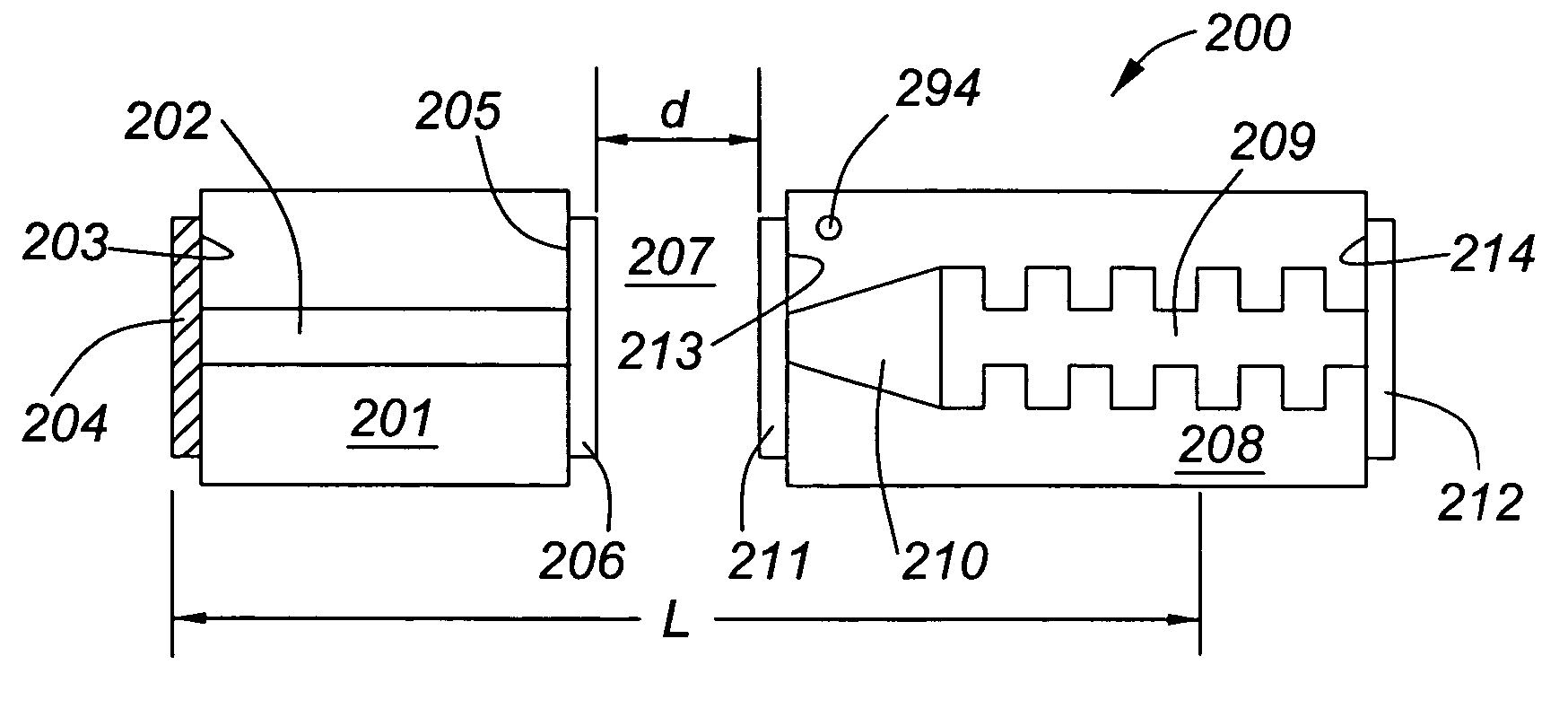
[0103]The first embodiment, shown in FIG. 4, is an external-cavity laser 200 comprising a gain medium in the form of a chip 201 having an active waveguide region 202 which can be defined as a ridge or buried waveguide, for example. The back facet 203 of the gain chip 201 is coated or terminated by a high reflectivity mirror 204 that is integral to the gain chip 201. The front facet 205 of chip 201 is coated by an optical grade antireflection coating 206. The requirements of the antireflection coating will be explained below. The gain chip 201 is brought within close proximity (i.e. butt-coupled) to a plasmon-polariton grating chip 208 through an intervening medium 207 of length d. The intervening medium 207 may be air or a material of refractive index n, for example a suitable epoxy resin.
[0104]The plasmon-polariton grating chip 208 contains a plasmon-polariton grating 209 and a mode converting element 210 which preferably, but not necessarily, takes the form of an adiabatic taper. ...
second embodiment
[0107]A second embodiment, shown in FIG. 5, comprises an external-cavity laser 220 identical to the laser 200 presented in FIG. 4 except that the mode conversion portion is transferred from the plasmon-polariton grating chip 208 to the gain chip 201. Thus, in the laser 220, shown in FIG. 5, the mode matching is provided as part of the waveguide 202. The mode conversion means, or expansion means in this case, is a tapered strip portion 222 for example. The mode matching can also be provided by a passive taper positioned away from the gain region, say in a plane longitudinally parallel to, and spaced from, waveguide 202 with broadside coupling provided therebetween.
[0108]The transition piece 222 could also be implemented as a small rib waveguide structure disposed on top of a larger one such that the mode transitions adiabatically between them, as disclosed by Vawter et al. in U.S. Pat. No. 6,229,947.
[0109]The alignment or butt-coupling of chips 201 and 208 is simplified in this laser...
fourth embodiment
[0113]A fourth embodiment, shown in FIG. 7, is an external-cavity laser 260 similar to those described with reference to FIGS. 4, 5 and 6 but which differs because it has no intervening mode conversion element 210, 222 or 242. In the laser 260, the waveguide 202 and the plasmon-polariton grating 209 on chips 201 and 208, respectively, provide sufficient modal overlap for successful coupling in the butt-coupled geometry shown, This can be achieved, for example, by designing the plasmon-polariton grating 209 and / or the waveguide 202 to match their mode sizes. The functioning of the laser 260 is the same as the first three embodiments, a cavity being formed between the mirror 204 and the plasmon-polariton grating 209 through a feedback mechanism provided by both the mirror and the plasmon-polariton grating. The effective optical path length of the cavity for this architecture is given by:
Leff=n202effL202+n207L207+n209effL209eff (26)
where n refers to the refractive index of the medium ...
PUM
 Abstract
Description
Claims
Application Information


