Piezoelectric sensor and input device including same

a technology of piezoelectric sensor and input device, which is applied in the direction of force measurement using piezo-resistive materials, instruments, fluid pressure measurement, etc., can solve the problems of complex structure, impaired durability, and difficulty in dealing with simultaneous multipoint contact, and achieves improved piezoelectric properties, improved piezoelectric properties, and excellent heat resistance.

Inactive Publication Date: 2006-12-26
NAT INST OF ADVANCED IND SCI & TECH
View PDF26 Cites 75 Cited by
  • Summary
  • Abstract
  • Description
  • Claims
  • Application Information

AI Technical Summary

Benefits of technology

[0039]Conversely, the piezoelectric sensor of the present invention has the pair of transparent conductor films opposed to each other with the piezoelectric element interposed therebetween. When one of the pair of the transparent substrates is subjected to outside pressure, the piezoelectric element takes a charge. The charge is detected by the transparent conductor films, so that the outside pressure is detected. Therefore, the transparent conductor films do not need to come into contact with each other, so that a flaw can be prevented from occurring due to contact. Moreover, the transparent conductor films do not need to be deformed, so that a piezoelectric sensor having an excellent durability as compared with the conventional arrangements can be provided.
[0087]With this arrangement, when different positions in the thin-film piezoelectric sensor are subjected to different stresses or pressures, different stresses are generated by different electrodes, so that different charges and voltages are generated on the different electrodes. In case of a cantilever-type and diaphragm-type piezoelectric sensor, there is a situation where it is effective in terms of sensitivity to detect a stress difference in the substrate provided with a piezoelectric thin film (i.e., a difference between the electrodes). Particularly, in case of detecting a shear stress, not a bending stress, in the cantilever-type piezoelectric sensor, it becomes possible to detect a difference with a hardware device, thereby achieving high-sensitivity detection without restrictions placed on a dynamic range of an amplifier.

Problems solved by technology

As a result, the resistance-film transparent input device raises such problems that: the transparent conductor films are flawed by coming into contact with each other, and durability is impaired because the transparent conductor films need to be deformed.
Therefore, the capacitance transparent input device and the analog-capacitor transparent input device raise such problem that they may malfunction when an electromagnetic noise is generated.
Moreover, the ultrasonic-surface-elastic-wave transparent input device and the infrared-scanning transparent input device raise such problem that they tend to have a complex structure and have difficulty in dealing with simultaneous multipoint contact.
However, because the peltiert element only has a function of simply generating a local temperature gradient, a cooling mechanism cannot be mounted on an outside remote from the piezoelectric body, so that the peltiert element cannot be applied to a part where a whole of the piezoelectric body becomes hot.
Therefore, as described above, because the conventional thin-film piezoelectric sensor cannot withstand high temperatures, an oscillation of a target object which reaches a high temperature is brought through an oscillation transmission bar to a remote low-temperature environment for measurement.
However, an oscillation such as an acoustic emission is attenuated due to a property of an oscillation transmission substance in the process or is mixed with an external redundant oscillation in the process of transmission, so that the oscillation of the target object cannot be measured sufficiently accurately.
However, lithium niobate is hard to make thinner and needs to be a monocrystalline body to obtain a piezoelectric property, thereby raising such problem that it is difficult to produce and process the sensor at low cost.
However, a substance whose crystal has a wurtzite structure (e.g., zinc oxide and aluminum nitride, described in the foregoing patent document) has difficulty in retaining a piezoelectric property, and it is impossible to stably improve a piezoelectric property only by a c-axis orientation of an axis of the crystal.
That is, a c-axis orientation is a factor necessary to improve a piezoelectric property but is not sufficient by itself to stably retain a piezoelectric property.
Experiment data shows that even when a substance having an excellent piezoelectric property can be produced, the substance is not reproducible.
This is because a piezoelectric sensor produced by the method of the foregoing patent document has a substrate and a piezoelectric layer provided directly thereon and therefore cannot stably align a direction of a dipole of a crystal of a piezoelectric element.
Even when a piezoelectric element which has a high dipole orientation degree is produced, it is difficult to obtain a piezoelectric element whose piezoelectric layer has a high dipole orientation degree.
This prevents the piezoelectric sensor from retaining a piezoelectric property and causes such problem that pressure cannot be detected satisfactorily.
However, lithium niobate, having a low processability, is hard to make thinner and needs to be used in a monocrystalline state.
Moreover, because a special method is required to form lithium niobate into an arbitrary shape, lithium niobate is limited in handling and therefore causes a problem with cost.
Further, lithium niobate has a problem with retention of a monocrystal.
In the worst case, a retention part may be damaged.
However, this inevitably results in a complex structure.
Thus, the conventional piezoelectric materials cause a pressure transmission structure to be complex, large and expensive and therefore cannot satisfy demand.

Method used


Image

  • Piezoelectric sensor and input device including same
  • Piezoelectric sensor and input device including same
  • Piezoelectric sensor and input device including same

Examples


example 1

[0138]An example of the piezoelectric sensor according to the First Embodiment will be described below.

[0139]A glass substrate with ITO (i.e., a glass substrate whose one surface is coated with ITO) was used as a transparent substrate and a transparent conductor film layer. The glass substrate with ITO had a thickness of 1 mm. Next, a thin film of aluminum nitride with a thickness of 1 μm serving as a transparent pressure-sensitive layer was formed on ITO of the glass substrate with ITO by a sputtering process.

[0140]Then, another glass substrate with ITO was prepared, and its ITO layer was bonded to the transparent pressure-sensitive layer of aluminum nitride with a cyanoacrylate-based binder.

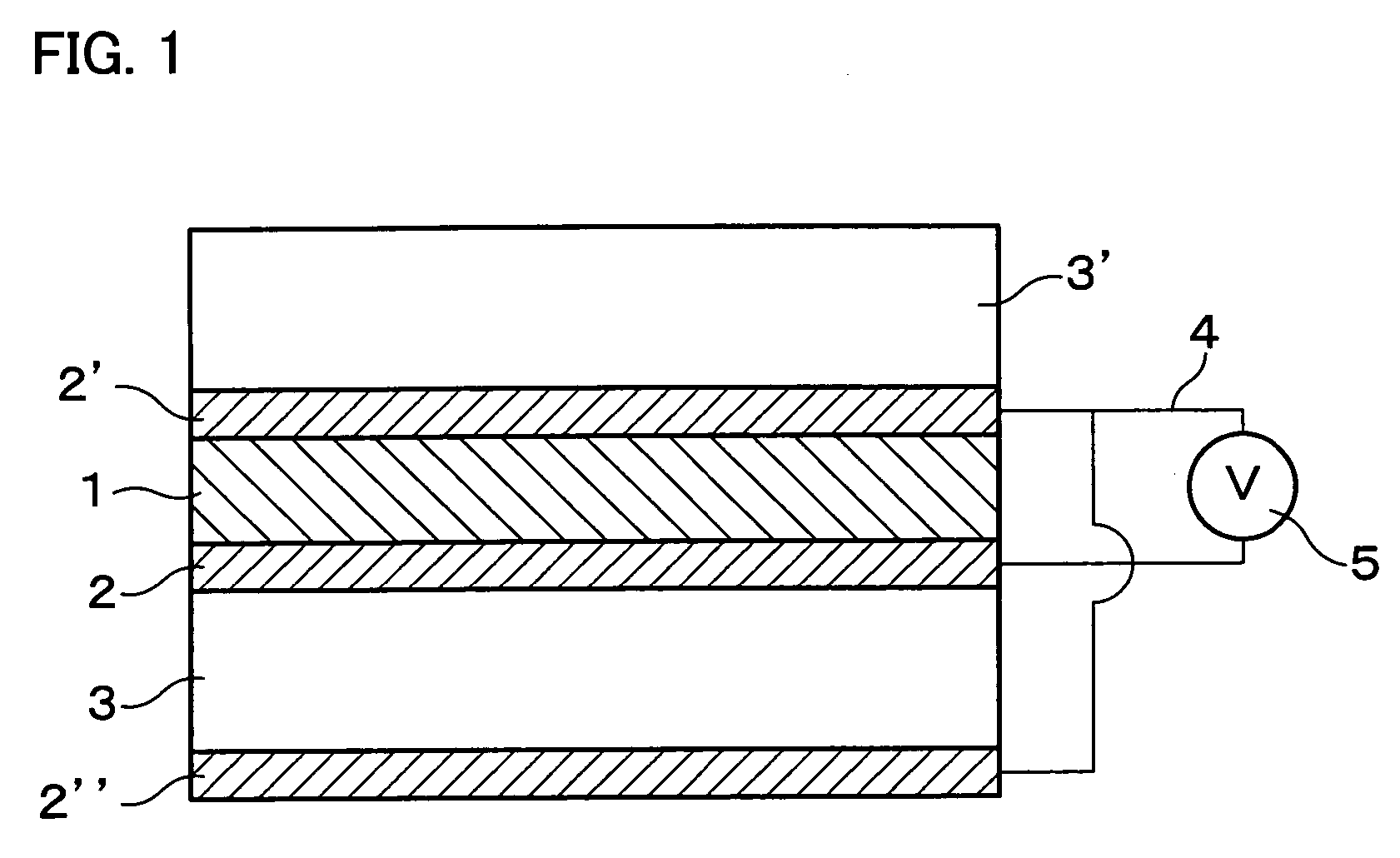
[0141]That is, the piezoelectric sensor of the present invention was made of a glass substrate (transparent insulative substrate layer), ITO (a transparent conductor film layer), aluminum nitride (a piezoelectric element), ITO (a transparent conductor film layer), a glass substrate (transparent...

example 2

[0209]An example of the piezoelectric sensor according to the Third Embodiment will be described below.

[0210]A base layer of a circular aluminum thin film with a diameter of 3 mm was formed by a sputtering process on a surface of a quartz glass substrate with a diameter of 17 mm and a thickness of 1 mm. Further on the base layer, a piezoelectric thin film layer of an AlN (aluminum nitride) thin film with a thickness of about 1 mm was produced by a sputtering process.

[0211]An analysis of an X-ray diffraction pattern showed that the AlN has an excellent crystalline property and is oriented in a c-axis direction. Further, a dipole orientation degree of a piezoelectric layer was 92%.

[0212]Next, a circular aluminum electrode, serving as an upper electrode, with a diameter of 3 mm was produced by a sputtering process on a surface of the AlN so as to overlap a lower electrode.

[0213]FIG. 10 shows a result of an oscillation detection measurement by a compression-type thin-film piezoelectric ...


PUM

PropertyMeasurementUnit
thicknessaaaaaaaaaa
operating temperatureaaaaaaaaaa
combustion temperatureaaaaaaaaaa

Abstract

A piezoelectric sensor arranged so as to includes: a transparent piezoelectric element having a piezoelectric property; and a pair of transparent conductor film layers opposed to each other with the piezoelectric element therebetween, the transparent piezoelectric element and the transparent conductor film layers are formed between a pair of transparent substrates, opposed to each other, which serve as pressure transmission means. Consequently, the transparent piezoelectric sensor has an excellent durability. A piezoelectric sensor comprises a piezoelectric element with a piezoelectric property which is made of a piezoelectric material having no Curie point and has a dipole orientation degree of not less than 75%. Consequently, the piezoelectric sensor having an excellent durability and a simple structure is provided at low cost.

Description

[0001]This application is the US national phase of international application PCT / JP2003 / 012379 filed 26 Sep. 2003 which designated the U.S. and claims benefit of JP's 2002-289197, 2002-322301 and 2002-352567, dated 1 Oct. 2002, 6 Nov. 2002 and 4 Dec. 2002, respectively, the entire content of which is hereby incorporated by reference.TECHNICAL FIELD[0002]The present invention relates to a piezoelectric sensor and an input device including the same. More particularly, the present invention relates to a piezoelectric sensor for detecting physical quantities such as acoustic emissions, pressure, oscillation, and acceleration in a high-temperature environment such as an inside of an internal combustion engine (or an inside of an internal combustion cylinder) and an inside of a plant such as an atomic power plant, or to a transparent piezoelectric sensor having a piezoelectric element formed between transparent conductor films opposite to each other (transparent electrodes), and to a tran...

Claims


Application Information

Patent Timeline
Patent Type & Authority Patents(United States)
IPC IPC(8): G01L9/00G01L1/18G01L23/22G06F3/033G06F3/041
CPCG01L1/16G01L9/008G01L23/222G06F3/0414
Inventor UENO, NAOHIROAKIYAMA, MORITOTATEYAMA, HIROSHI
Owner NAT INST OF ADVANCED IND SCI & TECH
Why Eureka
Try Eureka