Method of manufacturing an electronic component including an inter-line insulating layer and a conductor pattern

a manufacturing method and electronic component technology, applied in the field of electronic components, can solve the problems of large deviation of inductance values, difficult to have a narrow conductor width for the coil conductor, and extremely irregular size of the coil conductive pattern in terms of accuracy, so as to achieve accurate conductor pattern size and small direct current resistance value

Inactive Publication Date: 2007-01-09
MURATA MFG CO LTD
View PDF11 Cites 23 Cited by
  • Summary
  • Abstract
  • Description
  • Claims
  • Application Information

AI Technical Summary

Benefits of technology

[0009]To overcome the problems described above, preferred embodiments of the present invention provide a very small size electronic component having a small direct current resistance value in a conductor pattern and an extremely accurate conductor pattern size, and a production method thereof.

Problems solved by technology

However, according to this screen printing method, the size of the coil conductive pattern is extremely irregular in terms of the accuracy.
In addition, the deviation of the inductance values is large and it is difficult to have a narrow conductor width for the coil conductor.
However, according to this method, it is difficult to have a thick coil conductor pattern thickness compared with the screen printing method, and thus, it is difficult to produce an inductor with a high Q value.
However, due to a high production cost caused by a large number of manufacturing and processing steps required by the semi-additive process, a method of using a photosensitive conductive paste is preferable.
Therefore, even in the case of using a photosensitive conductive paste in the conventional method, a problem occurs in that the line width of the coil conductor pattern becomes small so as to have a large conductor loss, and thus, the Q value is lowered.
Moreover, since the limit of the resolution of a photosensitive conductive paste in the thickness direction has an aspect ratio of 1 (after development), it is difficult to have a thicker photosensitive conductive paste film.

Method used


Image

  • Method of manufacturing an electronic component including an inter-line insulating layer and a conductor pattern
  • Method of manufacturing an electronic component including an inter-line insulating layer and a conductor pattern
  • Method of manufacturing an electronic component including an inter-line insulating layer and a conductor pattern

Examples


Embodiment Construction

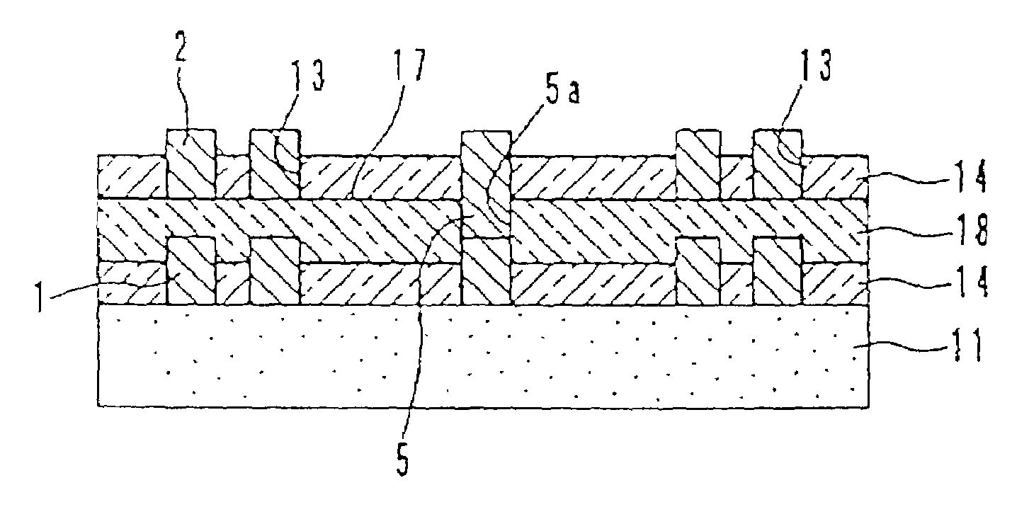
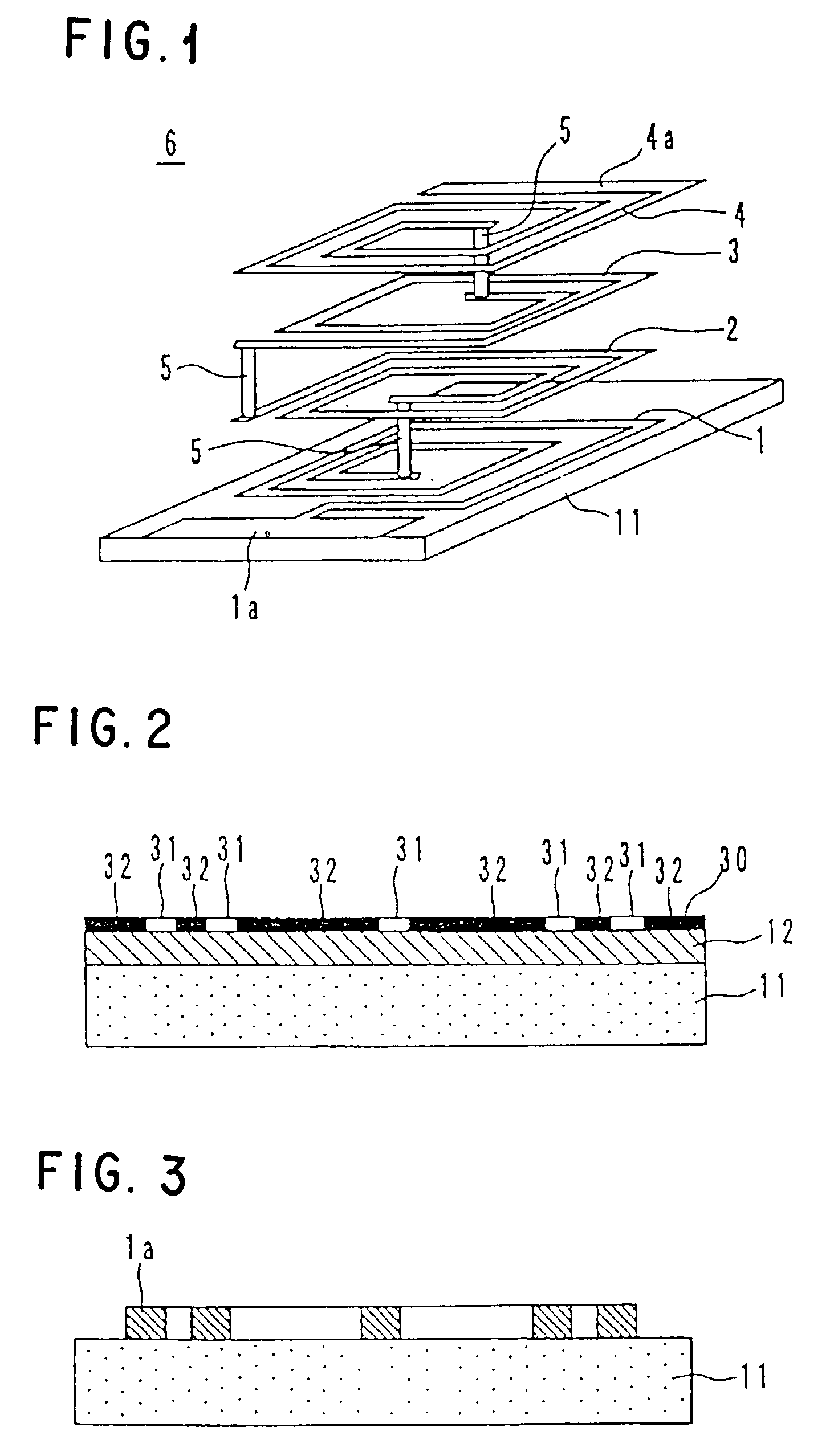
[0047]Hereinafter preferred embodiments of an electronic component according to the present invention and a method of manufacturing thereof will be explained with reference to the accompanying drawings. Although examples of an inductor will be explained as the electronic component, the present invention is not limited to the inductor but can be a strip line component, or other electronic component.

[0048]As shown in FIG. 1, an inductor 6 includes an insulating substrate 11 and spiral coil conductor patterns 1 to 4 provided on the insulating substrate 11. The insulating substrate 11 is made of a dielectric substance, an insulating material, or other suitable material. The coil conductor patterns 1 to 4 are connected electrically in series by via holes 5.

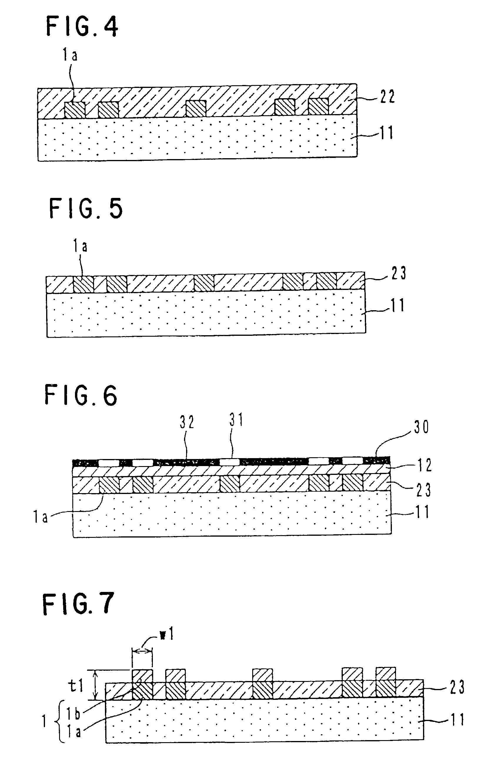
[0049]A method of manufacturing the multi-layer spiral inductor 6 will be explained with reference to FIGS. 2 to 12. Although the inductor 6 is manufactured using a mother substrate provided with a plurality of inductors for mass-produ...


PUM

PropertyMeasurementUnit
aspect ratioaaaaaaaaaa
photosensitiveaaaaaaaaaa

Abstract

A small size electronic component has a small direct current resistance value of a conductor pattern and minimal dimensional irregularity of a conductor pattern. In order to form such a component, a photosensitive conductive paste applied on a ceramic substrate and is then exposed through a photo mask and developed so as to form a lower conductor pattern layer of a coil conductor pattern. Then an insulating paste is applied on the ceramic substrate so as to cover the lower conductor pattern layer and the insulating paste is removed with a solvent until at least the upper surface of the lower conductor pattern layer is exposed so as to form an inter-line insulating layer. Furthermore, after applying a photosensitive conductive paste as a film, the exposure and development operation is conducted again while using the photo mask so as to form an upper conductor pattern layer on the lower conductor pattern layer.

Description

[0001]This application is a Divisional of U.S. patent application Ser. No. 09 / 350,038 filed Jul. 8, 1999, now U.S. Pat No. 6,555,913.BACKGROUND OF THE INVENTION[0002]1. Field of the Invention[0003]The present invention relates to an electronic component and a production method thereof. More specifically, the present invention relates to an electronic component such as a surface mount type inductor or strip line component, or other similar component, which is to be mounted on the surface of a pattern of a printed circuit board, and a production method thereof.[0004]2. Description of the Related Art[0005]A method of manufacturing a surface mount type inductor having a high Q value includes forming a coil conductive pattern on a ceramic mother substrate by a screen printing process with a large coil conductive pattern film thickness (large cross-sectional area) for having a small coil conductive pattern direct current resistance value (conductor loss) is commonly known. However, accord...

Claims


Application Information

Patent Timeline
Patent Type & Authority Patents(United States)
IPC IPC(8): H01L21/8234H01L21/8244H01F17/00H01F41/04H01L23/52H01L27/08H01L29/40H05K1/09H05K1/16H05K3/02H05K3/46
CPCH01F17/0013H01F41/043H01L27/08H05K3/4664H05K1/165H05K3/02H05K1/092
Inventor SASAKI, TOSHIYAUCHIYAMA, KAZUYOSHIKAWAGUCHI, MASAHIKOAMAYA, KEISHIROTAMEZAWA, EITA
Owner MURATA MFG CO LTD
Why Eureka
Try Eureka