Semiconductor device and method for manufacturing the same

Inactive Publication Date: 2007-01-16
PANNOVA SEMIC
View PDF22 Cites 10 Cited by
  • Summary
  • Abstract
  • Description
  • Claims
  • Application Information

AI Technical Summary

Benefits of technology

[0020]An object of the present invention is to solve these problems in the prior art insulating film in the thickness direction. Therefore, despite the reduced thickness of the gate insulating film, it is possible to prevent the diffusion of d

Problems solved by technology

The diffusion of boron is called “boron penetration”, and causes various problems in the transistor such as a substantial variation in the threshold voltage and a deterioration of the driving ability.
Furthermore, reducing the thickness of the gate insulating film also causes an increase in the gate leakage current through the gate insulating film.
As described above, if a thermal oxide film is used for the gate insulating film, it is no longer possible to suppress the boron penetration and the gate leakage current.
Moreover, it has also been found that in order to obtain an increased nitrogen concentration in an oxynitriding process using nitrogen monoxide or dinitrogen monoxide, it is necessary to increase the heat treatment temperature of the oxynitriding process, which is not suitable for the formation of a very thin gate insulating film.
However, when the thic

Method used


Image

  • Semiconductor device and method for manufacturing the same
  • Semiconductor device and method for manufacturing the same
  • Semiconductor device and method for manufacturing the same

Examples


first embodiment

[0062]The first embodiment of the present invention will now be described with reference to the drawings.

[0063]FIG. 1A to FIG. 1C and FIG. 2A to FIG. 2C are cross-sectional views sequentially illustrating the steps of a method for manufacturing a semiconductor device according to the first embodiment of the present invention.

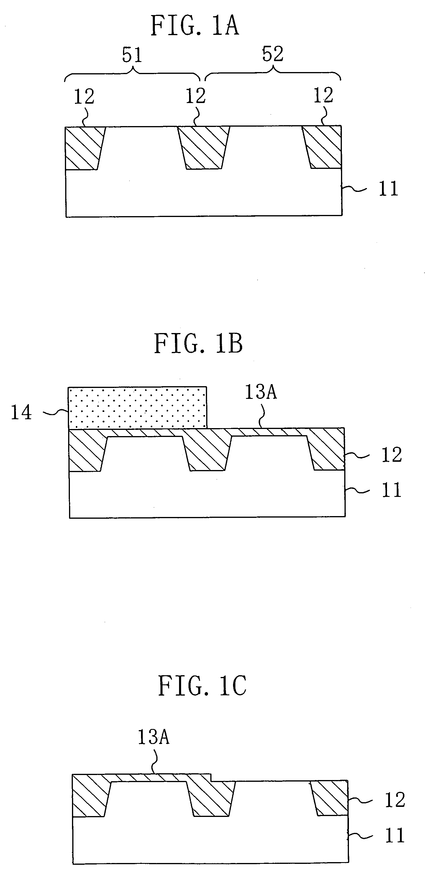
[0064]First, as illustrated in FIG. 1A, a semiconductor substrate 11 is prepared. For example, the semiconductor substrate 11 includes, in an upper portion thereof, an epitaxial layer (not shown) having a thickness of about 5 μm and made of P-type silicon whose specific resistance is about 11 Ωcm to 14 Ωcm, and the semiconductor substrate 11 has a specific resistance of about 0.01 Ωcm to 0.02 Ωcm. Then, a device isolation region 12, which is a shallow trench isolation, is formed in an upper portion of the semiconductor substrate 11. The device isolation region 12 partitions the principal surface of the semiconductor substrate 11 at least into a first device form...

second embodiment

[0097]The second embodiment of the present invention will now be described with reference to the drawings.

[0098]FIG. 8A to FIG. 8D are cross-sectional views sequentially illustrating the steps of a method for manufacturing a semiconductor device according to the second embodiment of the present invention.

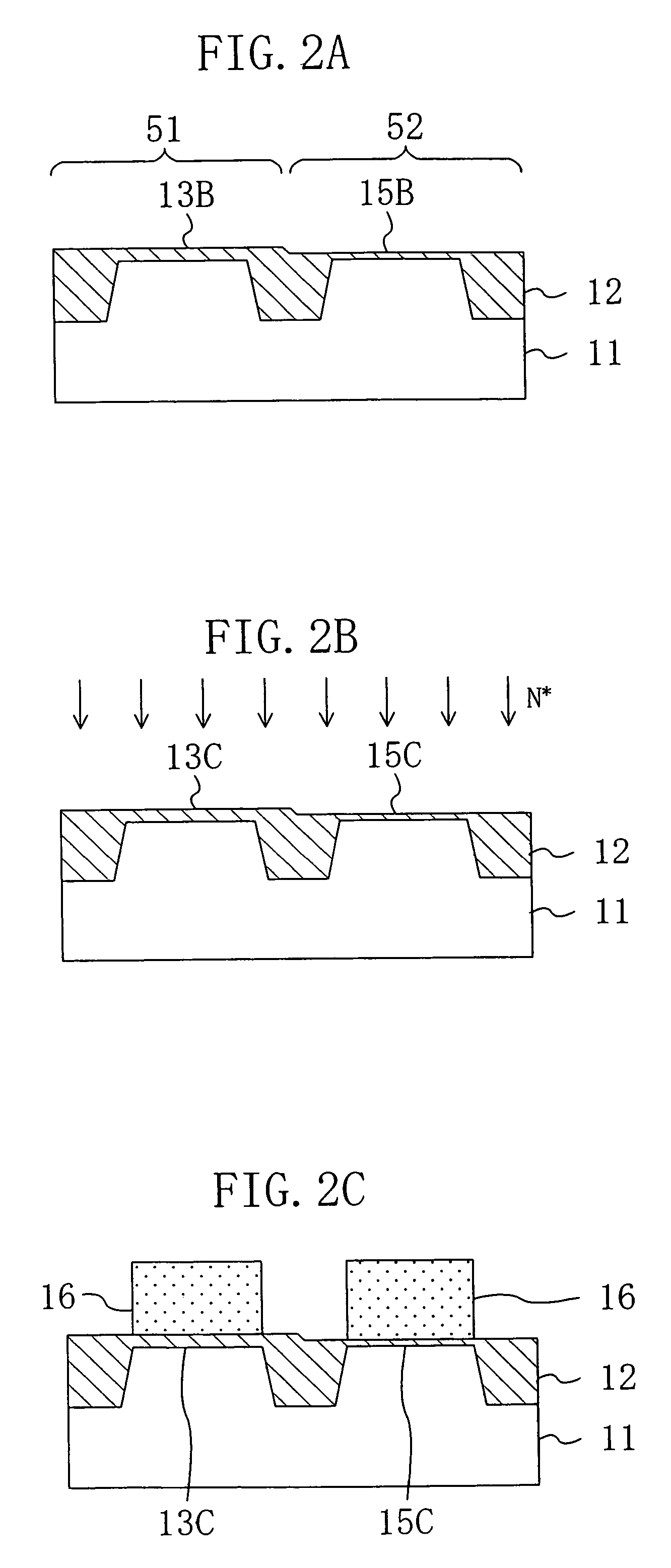
[0099]First, a device isolation region 22, which is a shallow trench isolation, is formed in an upper portion of a semiconductor substrate 21 made of P-type silicon. The device isolation region 22 partitions at least the first device forming region 51 and the second device forming region 52 from each other. Then, although not shown, a P-type well region and an N-type well region are formed in an upper portion of the semiconductor substrate 21, and a channel doping process is performed for adjusting the threshold voltage of the transistor. Then, the surface of the semiconductor substrate 21, in which the device isolation region 22 has been formed, is subjected to an SCl cleaning proc...

third embodiment

[0109]The third embodiment of the present invention will now be described with reference to the drawings.

[0110]FIG. 10A to FIG. 10C, FIG. 11A and FIG. 11B are cross-sectional views sequentially illustrating the steps of a method for manufacturing a semiconductor device according to the third embodiment of the present invention.

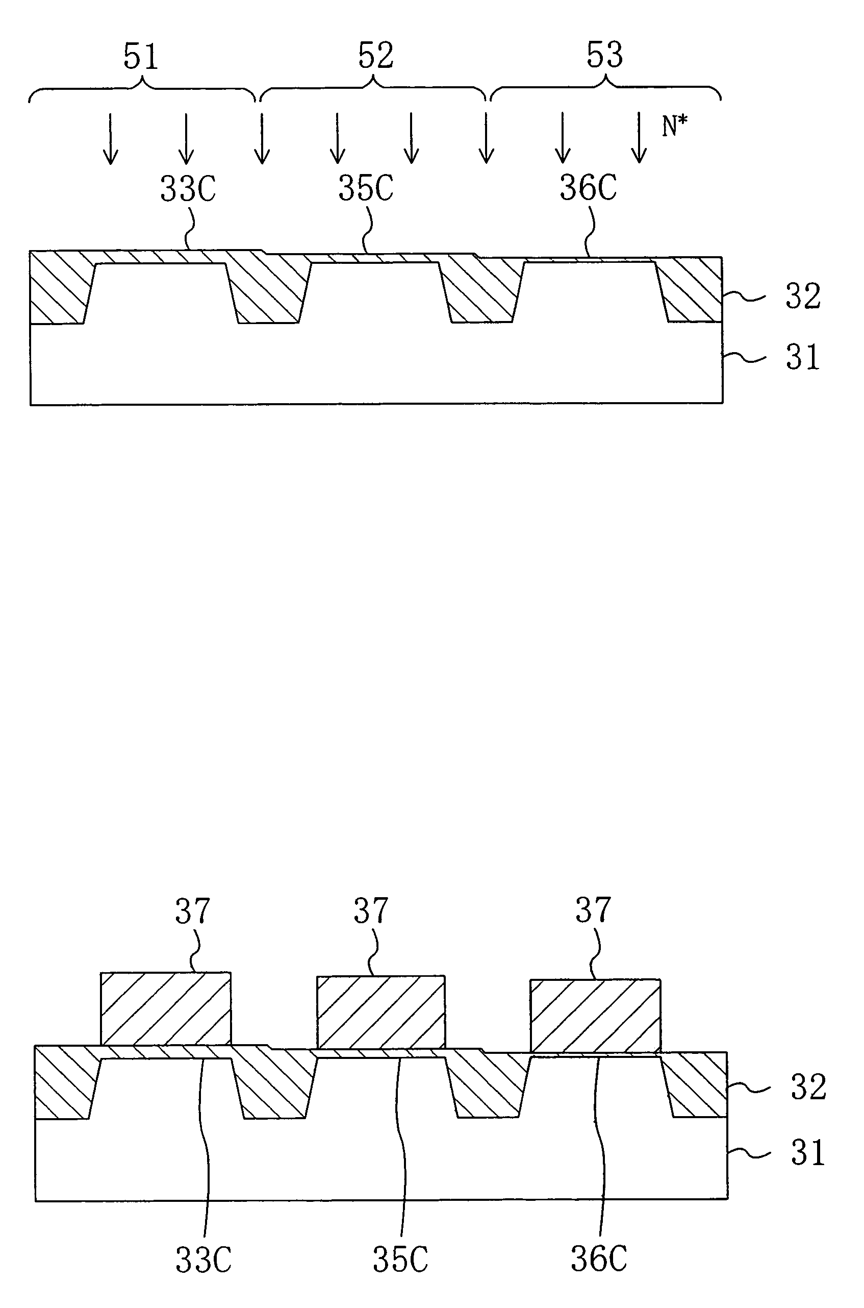
[0111]First, a device isolation region 32, which is a shallow trench isolation, is formed in an upper portion of a semiconductor substrate 31 made of P-type silicon. The device isolation region 32 partitions at least the first device forming region 51, the second device forming region 52 and a third device forming region 53 from one another. Then, although not shown, a P-type well region and an N-type well region are formed in an upper portion of the semiconductor substrate 31, and a channel doping process is performed for adjusting the threshold voltage of the transistor. Then, the surface of the semiconductor substrate 31, in which the device isolation regio...


PUM


Abstract

A semiconductor device includes a gate insulating film formed on a semiconductor substrate, and a gate electrode formed on the gate insulating film. Nitrogen is introduced into the gate insulating film, and the nitrogen concentration distribution thereof has a peak near the surface of the gate insulating film or near the center of the gate insulating film in the thickness direction. The peak value of nitrogen concentration in the gate insulating film is equal to or greater than 10 atm % and less than or equal to 40 atm %.

Description

BACKGROUND OF THE INVENTION[0001]The present invention relates to a semiconductor device and a method for manufacturing the same, and more particularly to a method for forming a gate insulating film used in a MIS transistor.[0002]A MOS transistor is a typical MOS device. For example, in a complementary MOS (CMOS) transistor, or the like, a high speed driving transistor, which is required to have a gate insulating film of a relatively thin thickness, and a high breakdown-voltage transistor, which is required to have a gate insulating film of a relatively thick thickness for handling input / output signals of a relatively high voltage, are formed on a single semiconductor substrate.[0003]The high speed driving transistor is required to have a gate insulating film having a thickness of about 1 nm to 3 nm, while it is strongly required to have a high reliability in resisting against dielectric breakdown and to have a low leakage current.[0004]A CMOS transistor employs a so-called “dual ga...

Claims


Application Information

Patent Timeline
IPC IPC(8): H01L29/76H01L21/265H01L21/28H01L21/8234H01L21/8238H01L29/51
CPCH01L21/28185H01L21/28202H01L21/823857H01L29/518H01L21/823462H01L21/26506Y10S438/981
Inventor YONEDA, KENJI
Owner PANNOVA SEMIC
Why Eureka
Try Eureka